

Rapid thermal process method and rapid thermal process device
a technology of rapid thermal process and thermal process device, which is applied in the direction of electric heating, laser beam welding apparatus, manufacturing tools, etc., can solve the problems of long process time of heating and cooling down and achieve the effect of reducing the thermal budget of the rapid thermal process, avoiding the risk of substrate breakage due to thermal stress, and improving the heating and cooling down time of the conventional chuck
- Summary
- Abstract
- Description
- Claims
- Application Information
AI Technical Summary
Benefits of technology
Problems solved by technology
Method used
Image

Examples
first embodiment
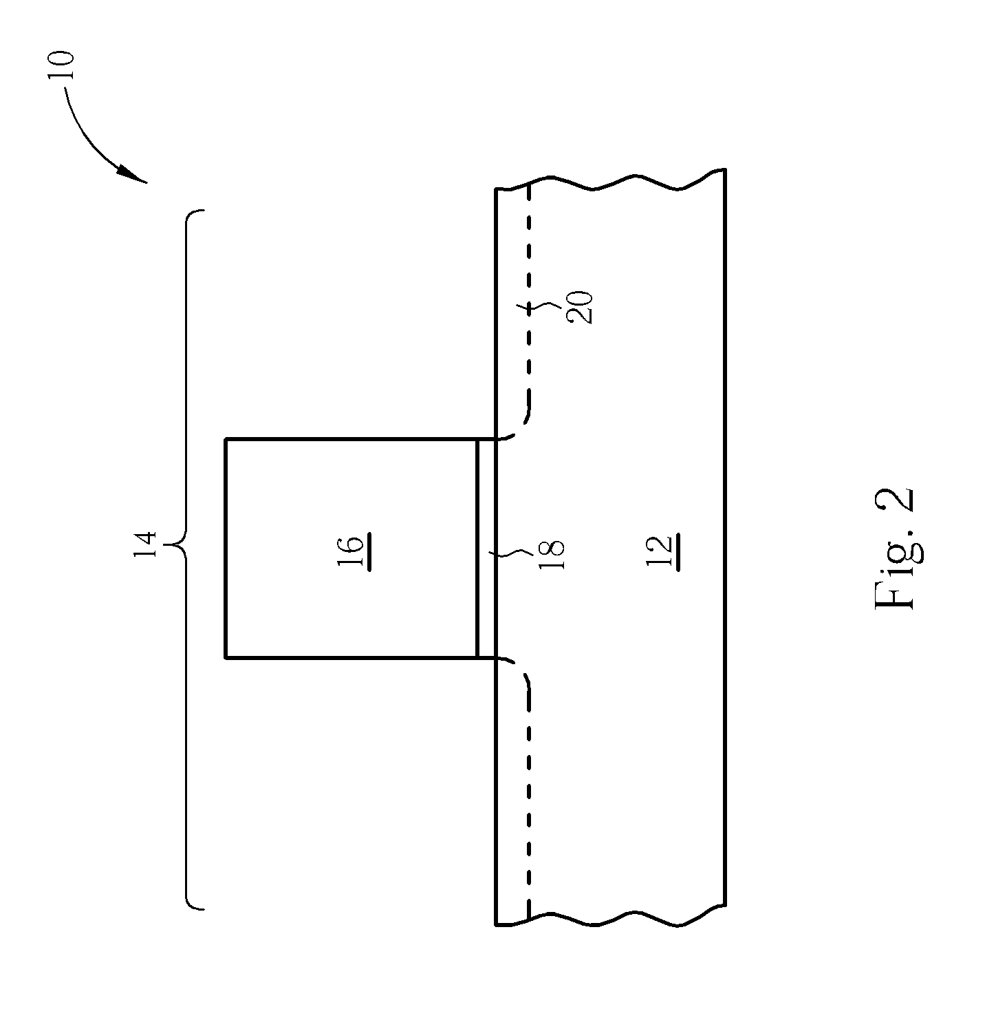
[0017]Please refer to FIG. 1 to FIG. 5, wherein FIG. 1 to FIG. 5 are schematic diagrams of the rapid thermal process method and rapid thermal process device according to the present invention. The rapid thermal process method of this embodiment may be applied to a fabrication process of the ultra shallow junction (USJ) of an MOS transistor of semiconductor wafers. First, with reference to FIGS. 1-2, a substrate 10 in need of a rapid thermal process is provided, wherein the substrate 10 may comprise a semiconductor wafer 12, such as a silicon wafer, comprising at least a MOS transistor regions 14 thereon. A gate 16 and a gate oxide layer 18 are formed on the surface of the substrate 10, and an ion implantation process has been performed to the substrate 10 so as to form the source / drain extension doping regions 20.
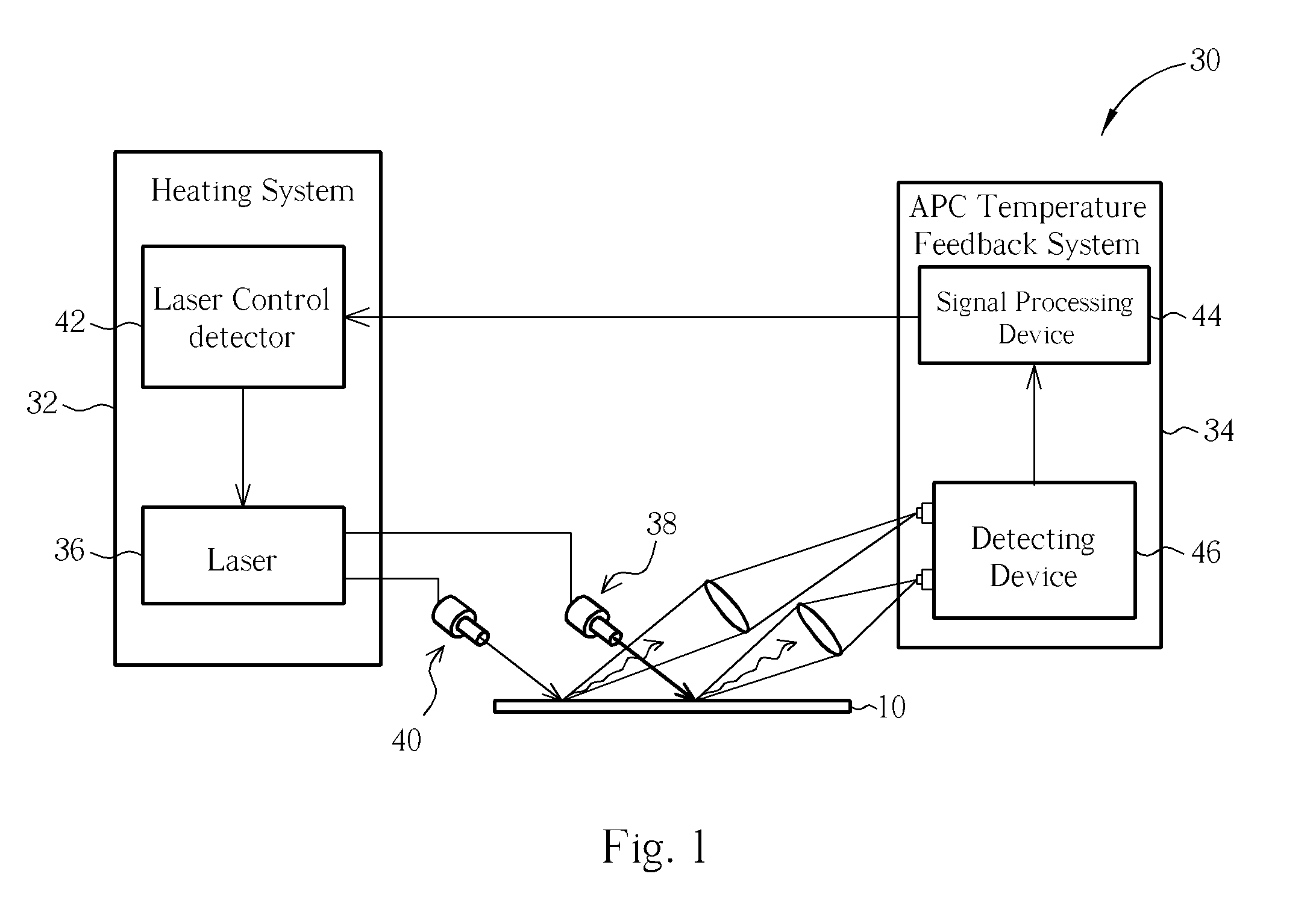
[0018]Then, the present invention rapid thermal process device 30 is utilized to perform a rapid annealing process to the substrate 10 for activating the dopants implanted ...
second embodiment
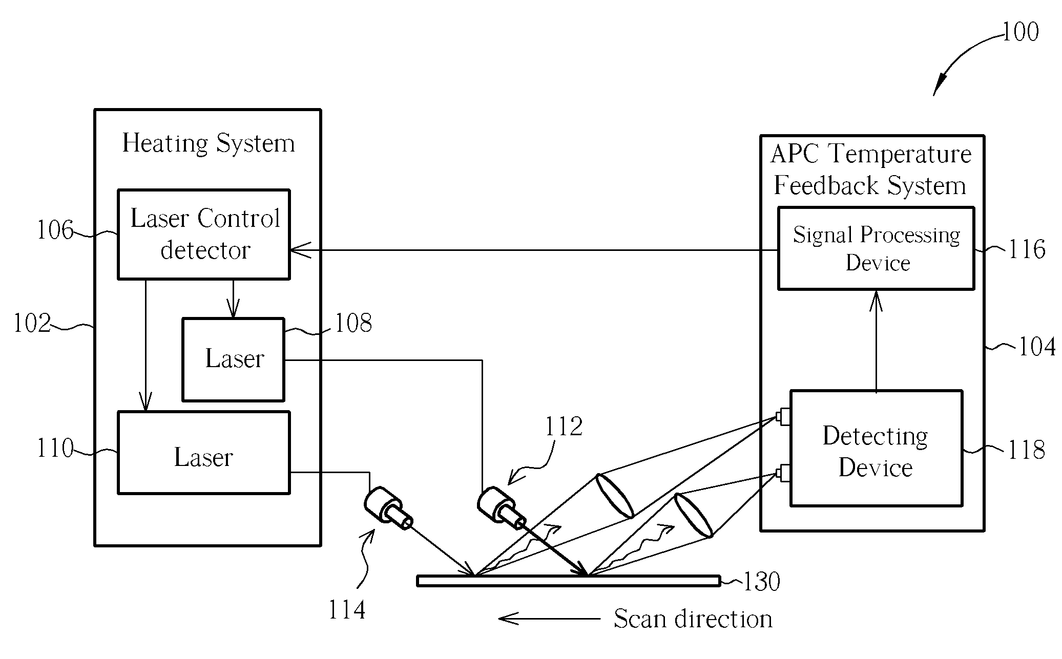
[0024]Please refer to FIG. 6, which is a schematic diagram of the rapid thermal process method and rapid thermal process device according to the present invention. The rapid thermal process device 100 of the present invention is used for performing a rapid thermal process of the substrate 130, and comprises a heating system 102 and a temperature feedback control system 104, wherein the temperature feedback control system 104 is an APC device. The heating system 102 comprises the first laser 108 and the second laser 110 that generate the first laser beam 112 and the second laser beam 114 respectively. The size or exposing range of the first laser beam 112 is larger than or equal to the size or exposing range of the second laser beam 114, and the exposing energy of the first laser beam 112 is lower than that of the second laser beam 114. The first and the second lasers 108, 110 may be controlled by a laser control detector 106 to have good stability, and the laser control detector 106...
third embodiment
[0026]With reference to FIG. 7, FIG. 7 is a schematic diagram of the rapid thermal process device of the present invention. In order to simplify the explanation, the numerals of FIG. 7 are the same as those of FIG. 6 for the same elements. As shown in FIG. 7, the heating system 102 comprises the first and the second lasers 108, 110 that generate the first laser beam 112 and the second laser beam 114 respectively so as to perform a pre-heating process and a rapid heating process to the substrate 130. The rapid heating process may be an msec laser non-melt annealing process or a melt laser annealing process. The temperature feedback control system 104 comprises a first detecting device 120 and a second detecting device 122 used for detecting the heating performances of the first laser beam 112 and the second laser beam 114 to the substrate 130 respectively. The first detecting device 120 and the second detecting device 122 may further provide an analysis function of the detecting resu...
PUM
| Property | Measurement | Unit |
|---|---|---|
| temperature | aaaaa | aaaaa |
| temperature | aaaaa | aaaaa |
| temperature | aaaaa | aaaaa |
Abstract
Description
Claims
Application Information