Array of Fet Transistors Having a Nanotube or Nanowire Semiconductor Element and Corresponding Electronic Device, For the Detection of Analytes
a technology of semiconductor elements and arrays, which is applied in the field of sensors, can solve the problems of limiting the ability of detecting a specific analyte in a mixture, affecting the detection efficiency of fet transistors, so as to improve the sensitivity, selectivity and response time.
- Summary
- Abstract
- Description
- Claims
- Application Information
AI Technical Summary
Benefits of technology
Problems solved by technology
Method used
Image

Examples
first embodiment
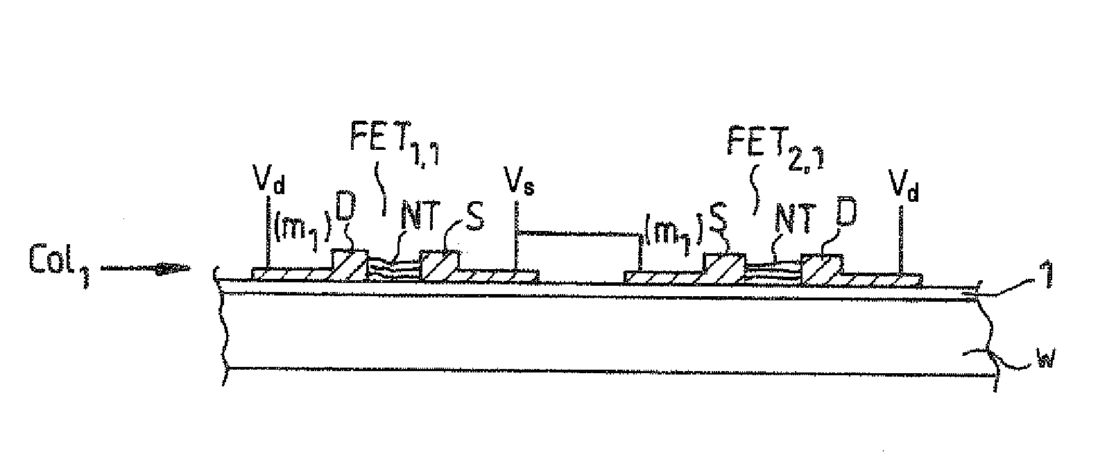
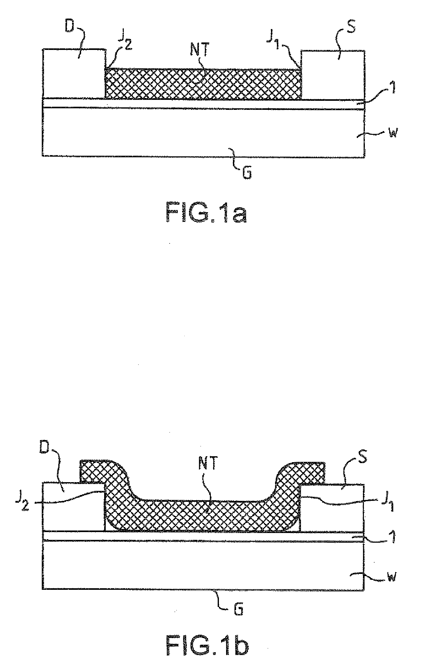
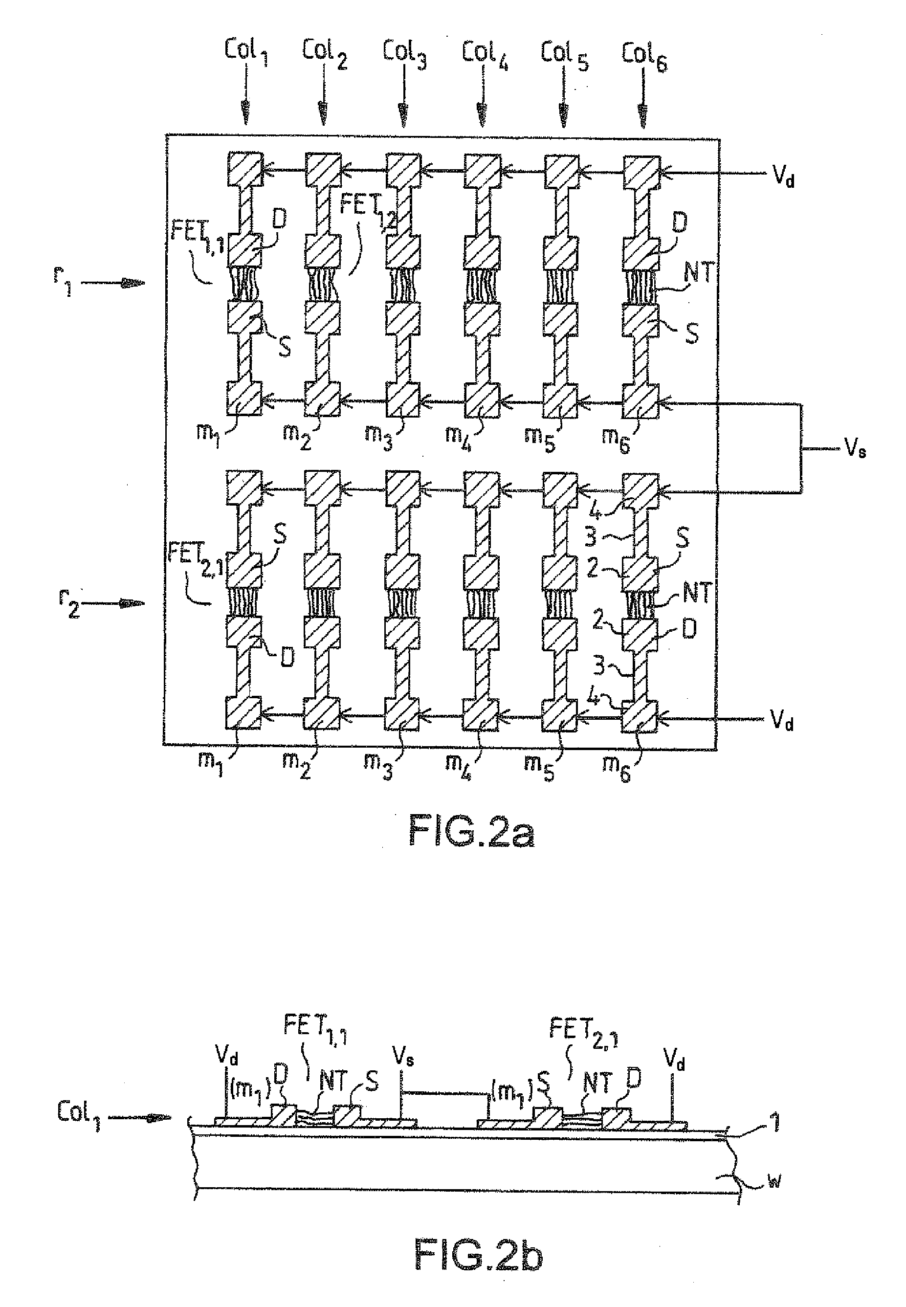
[0063]In a first embodiment illustrated in FIG. 1a, the electrodes are produced after the nanotube element NT has been deposited on the dielectric layer 1. For example, the electrodes are formed by deposition followed by self aligned etching on the nanotube element so that the junctions of the nanotube element with the electrodes lie in the plane of the nanotube element. This is the embodiment illustrated in FIG. 1a. The contact surface between the two materials forming the junction is essentially defined by the metal-covered surface of the nanotube.
second embodiment
[0064]In a second embodiment, illustrated in FIG. 1b, the source electrode S and drain electrode D are produced on the dielectric layer 1 (by deposition following by etching). The nanotube element NT is then deposited by partly covering the mesas of the electrodes. In this case, the contact surface between the two materials forming in each junction (metal / nanotube) is mainly the surface of the upper plane and of the sidewall of the mesa in contact with the nanotube element. This is the embodiment illustrated in FIG. 1b.
[0065]In the case in which the nanotube element is formed by a plurality of nanotubes, the nanotubes may contact the two electrodes or directly (2D array) or else by forming a chain, which enables them to be contacted, or else both.
[0066]It is in the region of the contact surface between the two materials of the junction that the dominent charge transfer mechanism takes place, and it is in this region that the analytes have the maximum influence.
[0067]An array compri...
PUM
| Property | Measurement | Unit |
|---|---|---|
| diameters | aaaaa | aaaaa |
| temperature | aaaaa | aaaaa |
| shape | aaaaa | aaaaa |
Abstract
Description
Claims
Application Information
 - R&D
- Intellectual Property
- Life Sciences
- Materials
- Tech Scout
- Unparalleled Data Quality
- Higher Quality Content
- 60% Fewer Hallucinations
Browse by: Latest US Patents, China's latest patents, Technical Efficacy Thesaurus, Application Domain, Technology Topic, Popular Technical Reports.
© 2025 PatSnap. All rights reserved.Legal|Privacy policy|Modern Slavery Act Transparency Statement|Sitemap|About US| Contact US: help@patsnap.com