Light emitting device

a light emitting device and light technology, applied in the direction of discharge tube luminescnet screen, discharge tube/lamp details, incadescent envelope/vessel, etc., can solve the problems of reducing light emitting efficiency, light emitting device exhibits poor color rendering characteristics, and lack of green ligh

Inactive Publication Date: 2008-09-04
SEOUL SEMICONDUCTOR
View PDF11 Cites 137 Cited by
  • Summary
  • Abstract
  • Description
  • Claims
  • Application Information

AI Technical Summary

Benefits of technology

[0010]The present invention is conceived to solve the problems of the conventional techniques as described above, and an aspect of the present invention is to provide a light emitting device capable of preventing light produced via wavelength conversion from being lost through absorption into a phosphor.
[0011]Another aspect of the present invention is to provide a light emitting device capable of preventing light produced via wavelength conversion from being lost through reentrance into an LED.
[0012]A further aspect of the present invention is to provide a light emitting device capable of preventing light, emitted from an LED for emitting long wavelength light, from being lost by an LED for emitting short wavelength light or by a phosphor.

Problems solved by technology

However, the technique of this disclosure realizes white light by mixing blue light and yellow light, and exhibits poor properties in view of color reproducibility and color rendering characteristics due to lack of light in the range of red color wavelengths.
On the other hand, white light can be realized by three LEDs including a blue LED, a green LED and a red LED, but in this case, the light emitting device exhibits poor color rendering characteristics irrespective of good color reproducibility due to narrow wavelength ranges of light emitted from the LEDs.
As a result, in the case where both the green phosphor and the red phosphor are contained in the light-transmitting resin, the light emitting device experiences a lack of green light and a reduction in light emitting efficiency due to a great amount of light lost therein.
Further, when red light enters the blue LED or an LED for short wavelength visible light, it can be lost due to reflection within these LEDs.

Method used


Image

  • Light emitting device
  • Light emitting device
  • Light emitting device

Examples


first embodiment

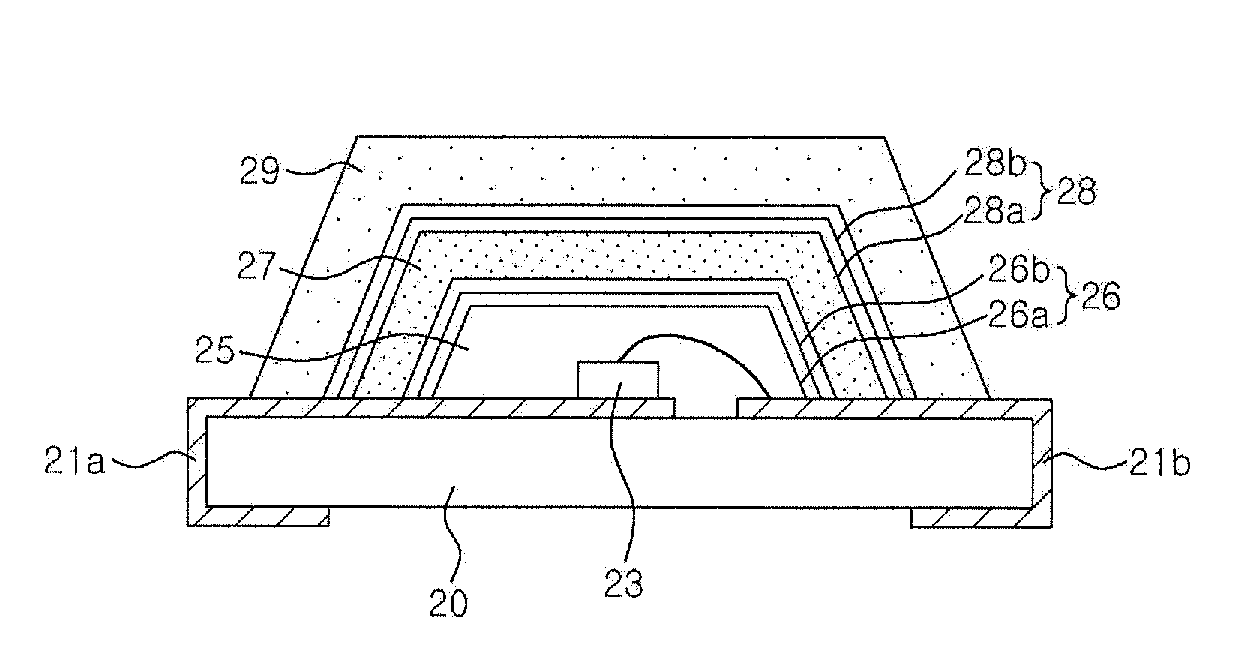
[0039]FIG. 1 is a cross-sectional view of a light emitting device including a plurality of wavelength conversion material layers according to the present invention.

[0040]Referring to FIG. 1, a light emitting diode (LED) 23 is mounted on a substrate 20. The substrate 20 may be a printed circuit board 20 that includes lead electrodes 21a and 21b in this embodiment. However, it can be selected from any substrate including a lead frame, a heat sink, a plastic package body, etc. without being limited to a particular substrate, as long as it permits a light emitting diode to be mounted thereon. The light emitting diode can be formed by growing GaAlInN-based compound semiconductor layers on a substrate formed of, for example, sapphire, SiC, spinel, or the like, and can emit ultraviolet rays or blue light as light of a first wavelength.

[0041]The LED 23 may be attached to the lead electrode 21a via conductive adhesives (not shown) and electrically connected to the lead electrode 21b through ...

second embodiment

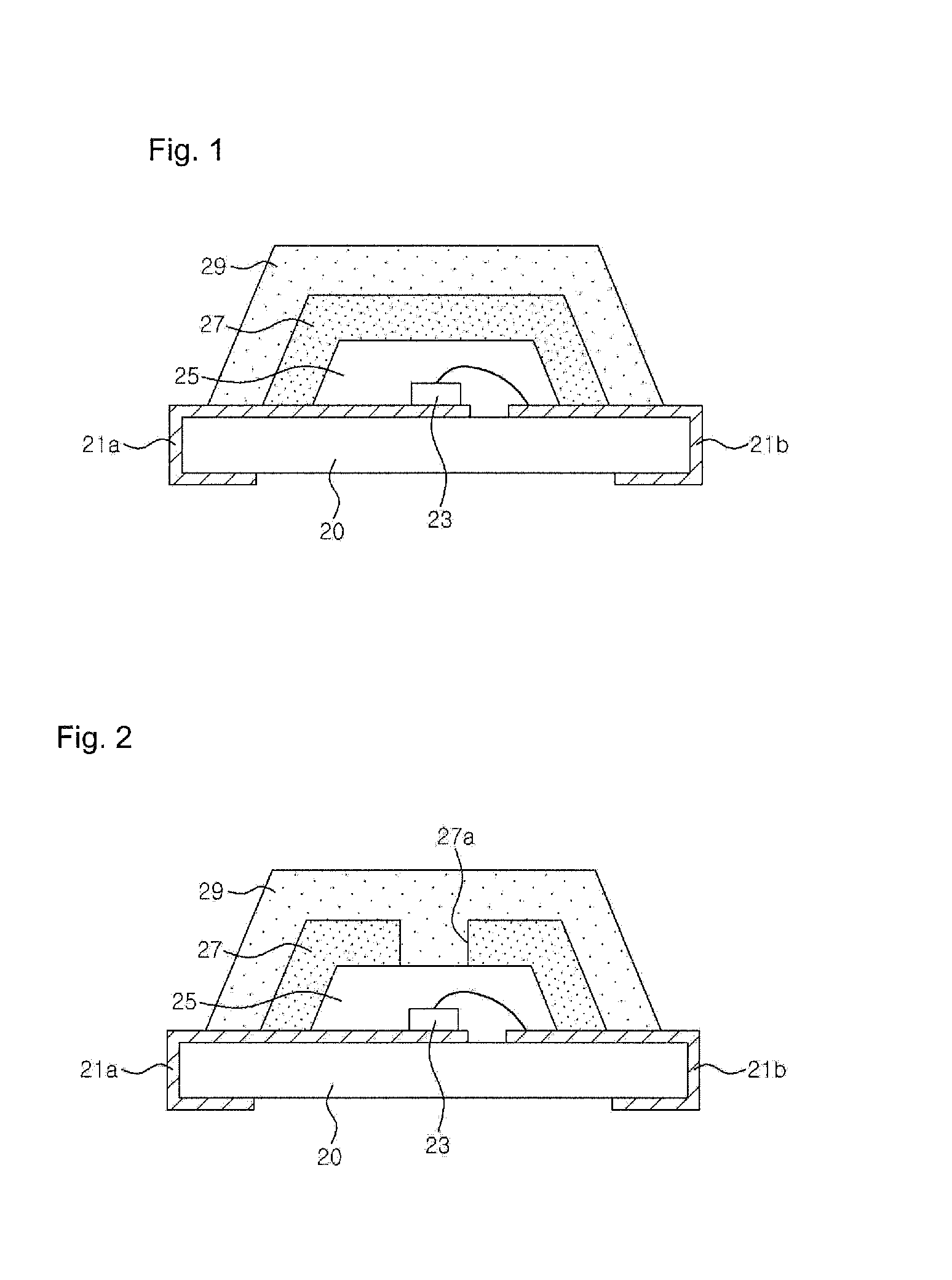
[0051]FIG. 2 is a cross-sectional view of a light emitting device including a plurality of wavelength conversion material layers according to the present invention.

[0052]Referring to FIG. 2, the light emitting device according to this embodiment has the same general configuration as that of the light emitting device illustrated in FIG. 1, except that a lower wavelength conversion material layer 27 of the second embodiment includes an opening 27a. The opening 27a exposes a transparent molding part 25 and is filled with an upper wavelength conversion material layer 29.

[0053]Hence, a fraction of light emitted from a LED 23 enters the upper wavelength conversion material layer 29 in the opening 27a without passing through the lower wavelength conversion material layer 27. As a result, the quantity of light exciting a phosphor in the upper wavelength conversion material layer 29 can be increased.

[0054]The lower wavelength conversion material layer 27 may have a plurality of openings 27a,...

third embodiment

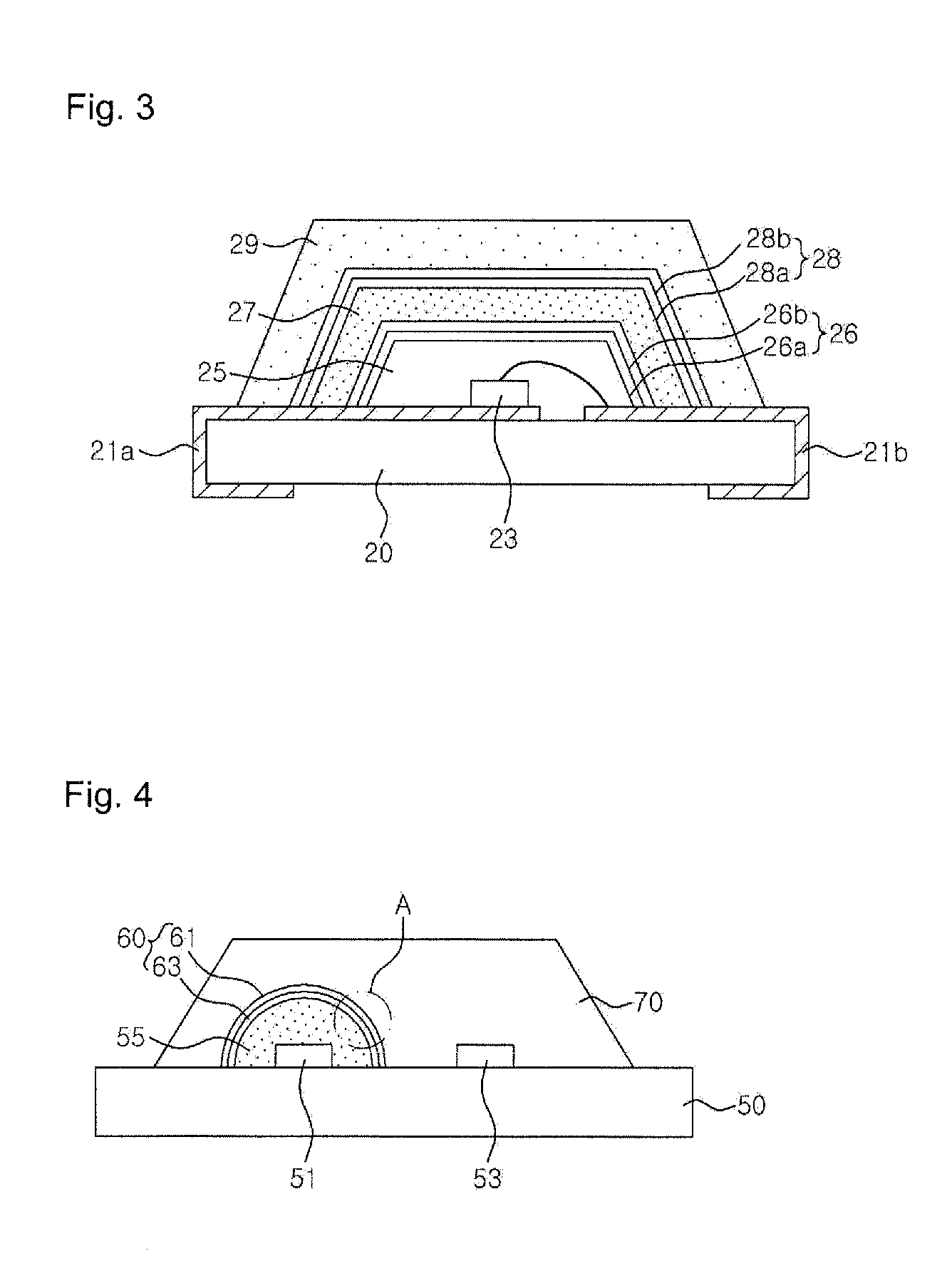
[0055]FIG. 3 is a cross-sectional view of a light emitting device including a plurality of wavelength conversion material layers according to the invention.

[0056]Referring to FIG. 3, the light emitting device of the this embodiment includes an LED 23 mounted on a substrate 20, a transparent molding part 25 disposed to enclose the LED 23, and lower and upper wavelength conversion material layers 27 and 29 on the transparent molding part 25. Herein, a lower dielectric multilayer reflection mirror 26 is formed between the transparent molding part 25 and the lower wavelength conversion material layers 27, and an upper dielectric multilayer reflection mirror 28 is formed between the lower wavelength conversion material layers 27 and the upper wavelength conversion material layer 29.

[0057]The lower dielectric multilayer reflection mirror 26 includes at least one pair of low- and high-refractivity dielectric layers 26a and 26b. Herein, the lower wavelength conversion material layer 27 has ...


PUM


Abstract

Disclosed herein is a light emitting device. The light emitting device includes a light emitting diode disposed on a substrate to emit light of a first wavelength. A transparent molding part encloses the LED, a lower wavelength conversion material layer is disposed on the transparent molding part, and an upper wavelength conversion material layer is disposed on the lower wavelength conversion material layer. The lower wavelength conversion material layer contains a phosphor converting the light of the first wavelength into light of a second wavelength longer than the first wavelength, and the upper wavelength conversion material layer contains a phosphor converting the light of the first wavelength into light of a third wavelength, which is longer than the first wavelength but shorter than the second wavelength. Light produced via wavelength conversion is prevented from being lost by the phosphor. Light emitting devices including a multilayer reflection mirror are also disclosed.

Description

BACKGROUND OF THE INVENTION[0001]1. Field of the Invention[0002]The present invention relates to a light emitting device, and more particularly to a light emitting device capable of preventing light, emitted from a light emitting diode or produced via wavelength conversion, from being lost within the light emitting device.[0003]2. Description of the Related Art[0004]Light emitting devices manufactured with compound semiconductor light emitting diodes can realize various colors and are used for various applications including lamps, electronic display boards, and displays. In particular, since the light emitting device can realize white light, it is used for general lighting and light sources of liquid crystal display panels.[0005]Generally, white light can be obtained by combination of a blue light emitting diode (LED) and phosphors, and one example of light emitting devices that realize white light based on the blue LED and YAG phosphor is disclosed in JP Patent Laid-open No. 2002-0...

Claims


Application Information

Patent Timeline
Patent Type & Authority Applications(United States)
IPC IPC(8): H01J1/62H01L33/32H01L33/50H01L33/56H01L33/62
CPCH01L33/44H01L33/46H01L33/504H01L2224/48091H01L2224/48227H01L2924/00014
Inventor CHOI, HYUCK JUNGPARK, KWANG II
Owner SEOUL SEMICONDUCTOR
Why Eureka
Try Eureka