Method of manufacturing oxide film and method of manufacturing semiconductor device

a manufacturing method and semiconductor technology, applied in the manufacturing process, superimposed coating process, liquid/solution decomposition chemical coating, etc., can solve the problems of difficult to obtain gate oxide film, difficult to deposit high-quality oxide film, adverse effect of oxide film quality

Inactive Publication Date: 2008-09-04
KK TOSHIBA
View PDF2 Cites 0 Cited by
  • Summary
  • Abstract
  • Description
  • Claims
  • Application Information

AI Technical Summary

Benefits of technology

[0012]The present invention is intended to provide not only a method of manufacturing at a low temperature an oxide film which is relatively free from damages and is applicable to a semiconductor device, but also a semiconductor device manufacturing method including the oxide film manufacturing method.
[0014]In accordance with a second aspect of the embodiment of the invention, there is provide a method of manufacturing an oxide film, including: lowering a resistance of a solution serving as an oxygen source; heating the solution to a room temperature or higher; applying a pressure of 5 MPa or higher to the solution; jetting the pressurized solution onto a substrate; and depositing an oxide film using the jetted high-pressure solution.

Problems solved by technology

However, it is difficult to deposit high quality oxide films since the oxide film and substrate are easily damaged by charged particles (ions, electrons, etc.) or electromagnetic waves (UV rays, x-rays, etc.).
However, since the surface of the thin substrate which is approximately 4 nm to 5 nm thick is oxidized only through the chemical reaction, the quality of the oxide film is adversely affected.
Therefore, it is very difficult to obtain a gate oxide film which is 10 nm or thicker and is applicable to a semiconductor device demanded at present.

Method used


Image

  • Method of manufacturing oxide film and method of manufacturing semiconductor device
  • Method of manufacturing oxide film and method of manufacturing semiconductor device
  • Method of manufacturing oxide film and method of manufacturing semiconductor device

Examples


example 1

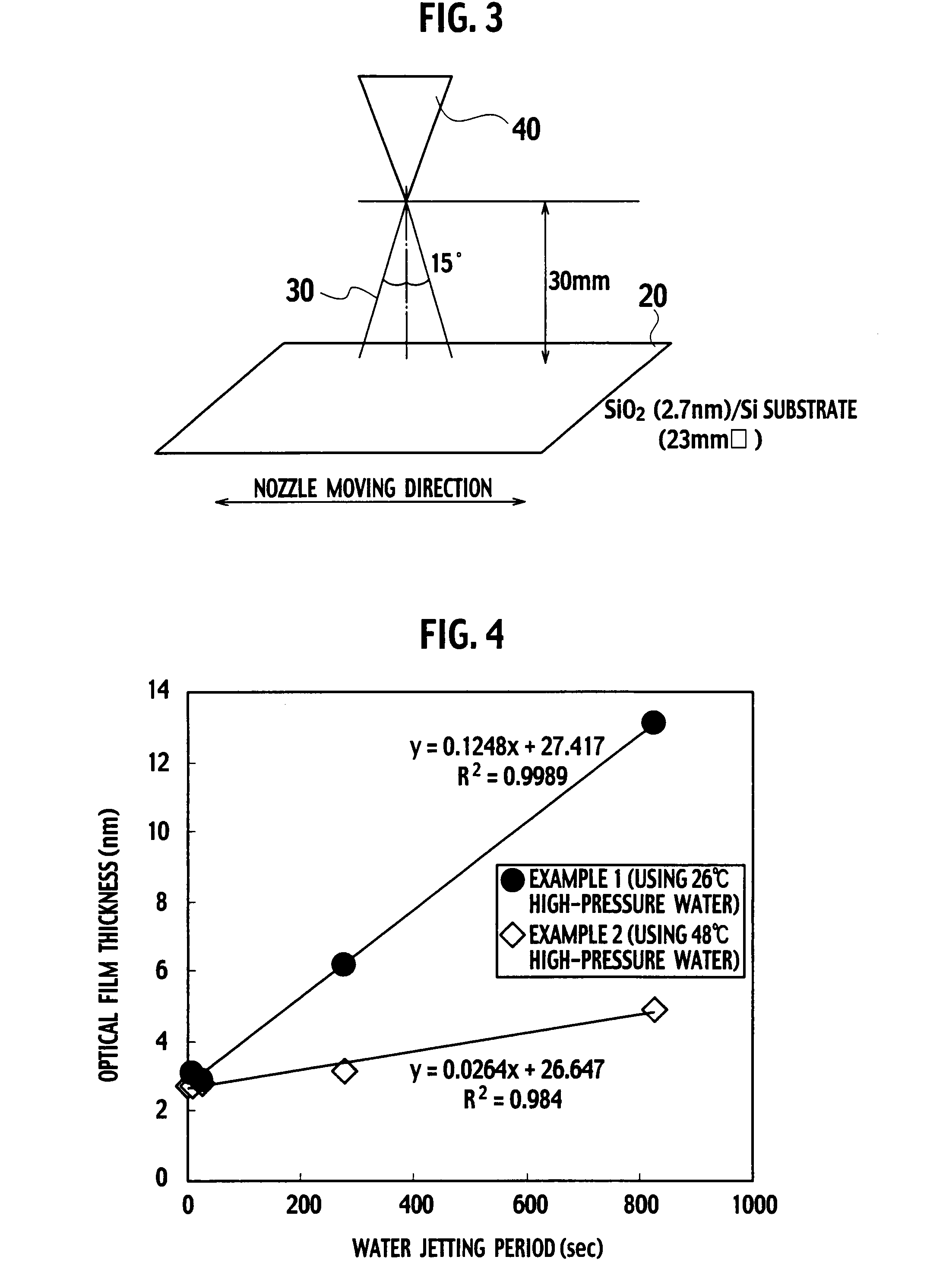
[0058]For convenience of the evaluation, an approximately 2.7 nm thick thermal oxide film is deposited on an n-type silicon wafer by thermal treatment at 900° C. The Si substrate has a specific resistance of 1 Ωcm to 2 Ωcm. The substrate is cleaned for approximately 20 minutes using an ultrasonic washing machine (MHz).

[0059]The oxide film is deposited on the thermal oxide film of the silicon wafer. High-pressure water 30 is prepared by dissolving CO2 gas of 5 mg / l in deionized water having the specific resistance of 18 MΩcm. The high-pressure water 30 has the specific resistance of 0.5 Ωcm and pH 5.3, and is 26° C.

[0060]As shown in FIG. 3, the high-pressure water 30 is substantially vertically jetted onto the silicon wafer 20 via the nozzle 40. The pressure of the high-pressure water 30 at the outlet of the nozzle 40 is 20 MPa, and a distance between the nozzle 40 and the silicon wafer 20 is 30 mm. The high-pressure water 30 diverges approximately 15 degrees via the nozzle 40.

[0061]...

example 2

[0062]In Example 2, the high-pressure water 30 is set to be 48° C. The remaining conditions are the same as those in Example 2.

Evaluation

[0063]FIG. 4 shows the relationship between the high-pressure water jetting period and the optical film thickness of the oxide films in Examples 1 and 2.

[0064]The optical film thickness is derived by measuring a single layer model of SiO2 (n=1.46) / Si (n=3.86) using an optical coating thickness gauge. When the high-pressure water temperatures are respectively 26° C. and 48° C. in Examples 1 and 2, the thickness of the oxide films are confirmed to increase in proportion to the jetting period. In other words, jetting of the high-pressure water is effective in manufacturing the oxide film with excellent controllability. The hotter the high-pressure water, the higher the oxidizing rate. When the high-pressure water is 48° C., the oxidizing rate is assumed to be approximately 0.75 nm / min.

[0065]FIG. 5A and FIG. 5B shows results of XPS (x-ray photoelectr...

further embodiment

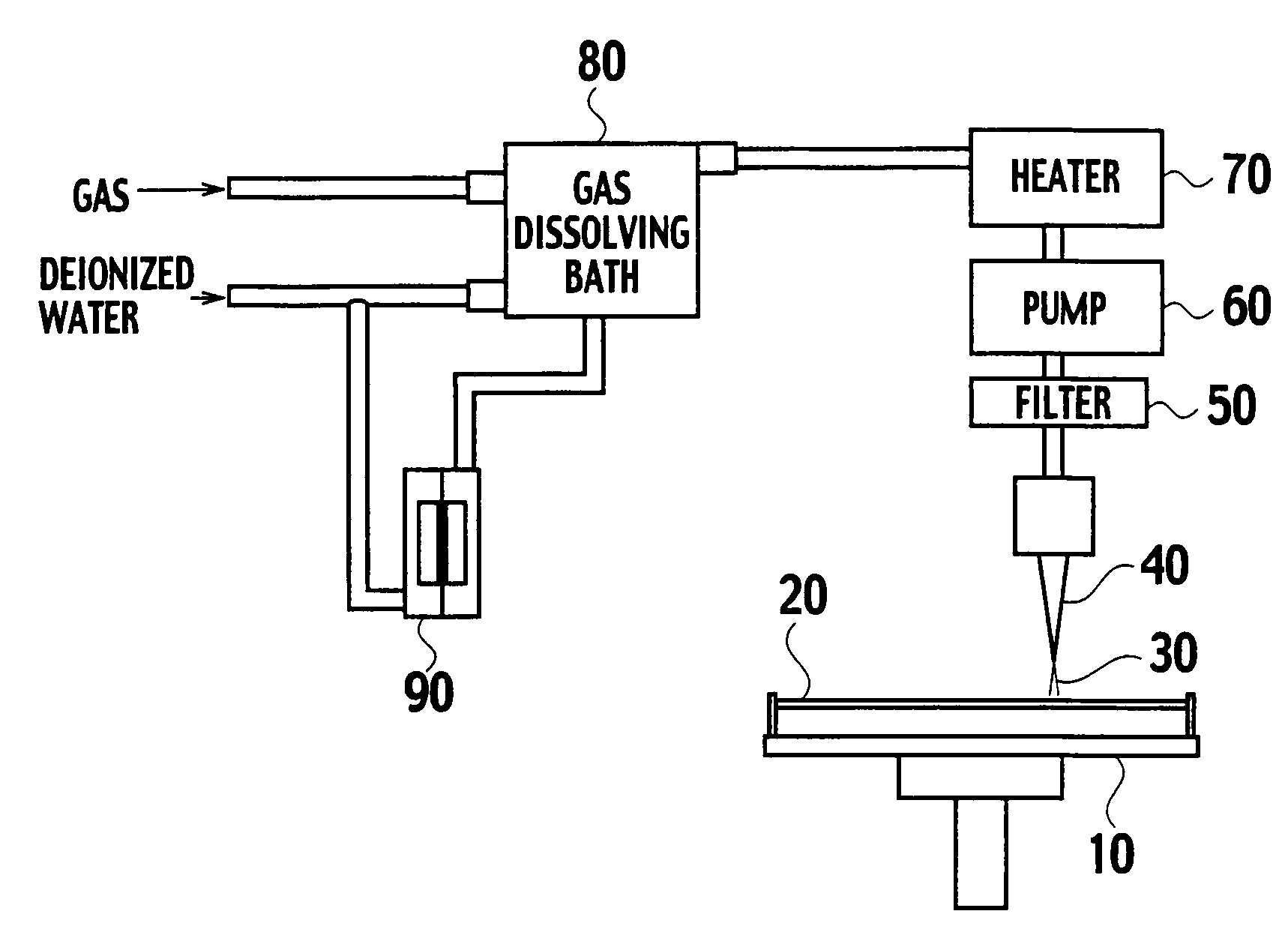
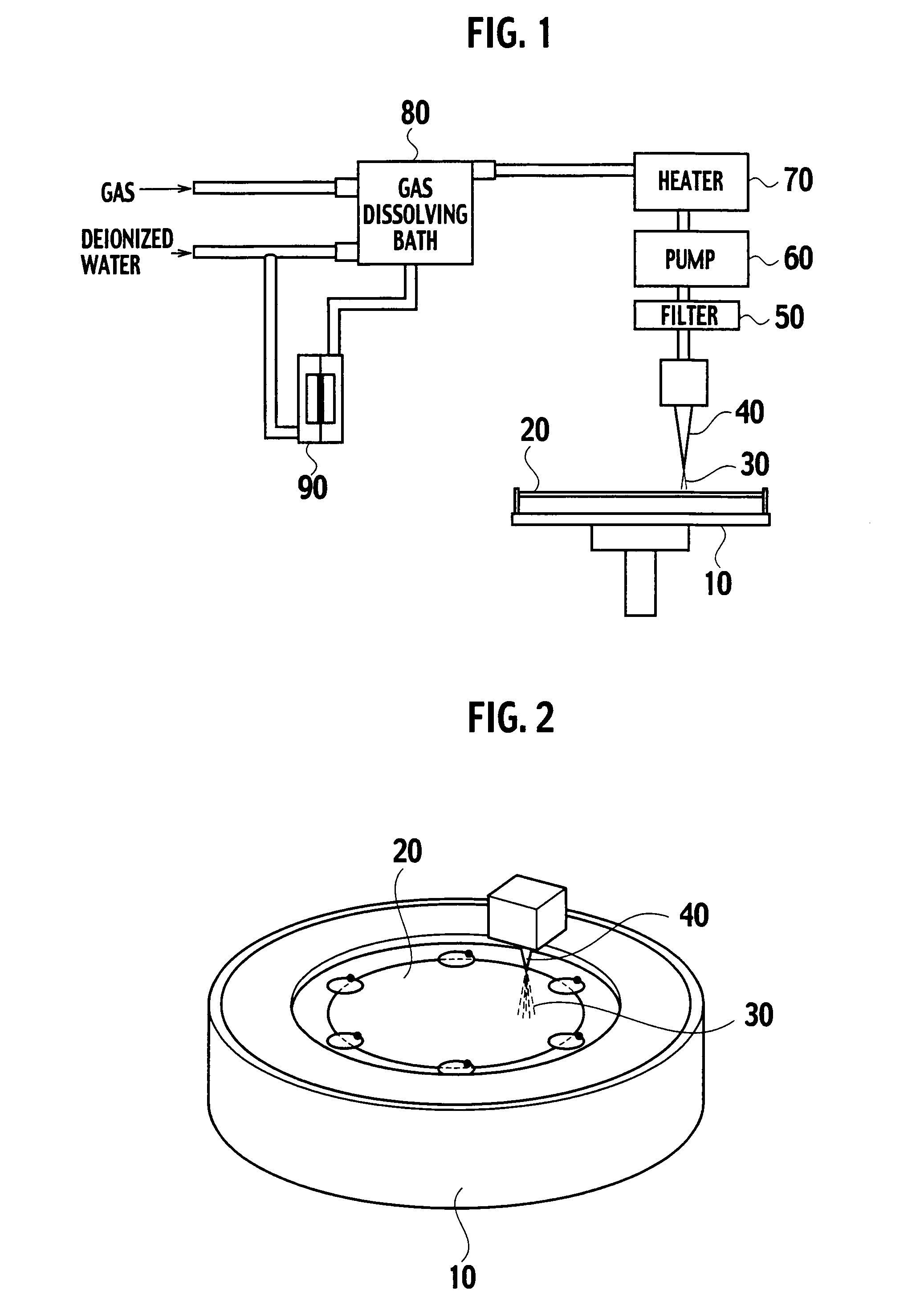
[0090]A modified example of the substrate treating unit (shown in FIG. 1) is shown in FIG. 12. The substrate heating unit includes a cleaning device 200, and can produce and clean oxide films.

[0091]The cleaning device 200 includes a nozzle 140 supplying a cleaning agent onto a silicon wafer 20. Deionized water is supplied from the feeder of the substrate treating unit, and the gas dissolving bath 80 of the substrate treating unit is also utilized. A chemical dispenser 110B is provided between the gas dissolving bath 80 and the nozzle 140, thereby supplying a proper amount of cleaning agent such as an etchant into an aqueous solution in which CO2 gas is dissolved, via a liquid mass flow controller 120B.

[0092]If necessary, a submerged particle counter 130 may be provided in a supply tube. The substrate stand 10 of the substrate treating unit is also used for the cleaning. In other words, cleaning of the substrate and deposition of the oxide film can be conducted in one unit.

[0093]The ...


PUM

PropertyMeasurementUnit
pressureaaaaaaaaaa
thickaaaaaaaaaa
pressureaaaaaaaaaa

Abstract

A method of manufacturing an oxide film includes jetting onto a substrate a high-pressure solution containing an oxygen source and having a pressure of 5 MPa, and forming an oxide film on the substrate using the jetted high-pressure solution.

Description

CROSS REFERENCE TO RELATED APPLICATIONS[0001]This application is a continuation of and claims the benefit of priority under 35 U.S.C. § 120 for U.S. Ser. No.: 11 / 233,024 filed Sep. 23, 2005 and under 35 U.S.C. § 119 from the Japanese Patent Application No. 2004-277,911 filed on Sep. 24, 2004; the entire contents of each of which is incorporated by reference herein.BACKGROUND OF THE INVENTION[0002]1. Field of the Invention[0003]This invention relates to a method of manufacturing an oxide film and a method of manufacturing a semiconductor device, and more particularly relates a method of manufacturing an oxide film on a substrate, and a semiconductor device manufacturing method which is applied to manufacturing a high quality oxide film at a low temperature.[0004]2. Description of the Related Art[0005]Oxide films have been widely applied to a variety of semiconductor devices, and should be relatively free from defects and have excellent interface states when used as gate oxide films f...

Claims


Application Information

Patent Timeline
Patent Type & Authority Applications(United States)
IPC IPC(8): H01L21/31B05D1/02
CPCH01L21/02238H01L21/31675H01L21/02255
Inventor KATSUMATA, HIROSHISAITO, MAKOTOFUJITA, HIROSHINISHIMURA, ERIKO
Owner KK TOSHIBA
Why Eureka
Try Eureka