Semiconductor device and method of manufacturing the same
a technology of thin metal film and resistor, which is applied in the direction of resistors, semiconductor devices, electrical equipment, etc., can solve the problems of difficult to achieve the required etching selectivity between an insulation film and a metal film, reduce the thickness of the thin metal film resistor, and reduce the resistance of the thin metal film. , the effect of high layout flexibility
- Summary
- Abstract
- Description
- Claims
- Application Information
AI Technical Summary
Benefits of technology
Problems solved by technology
Method used
Image

Examples
first embodiment
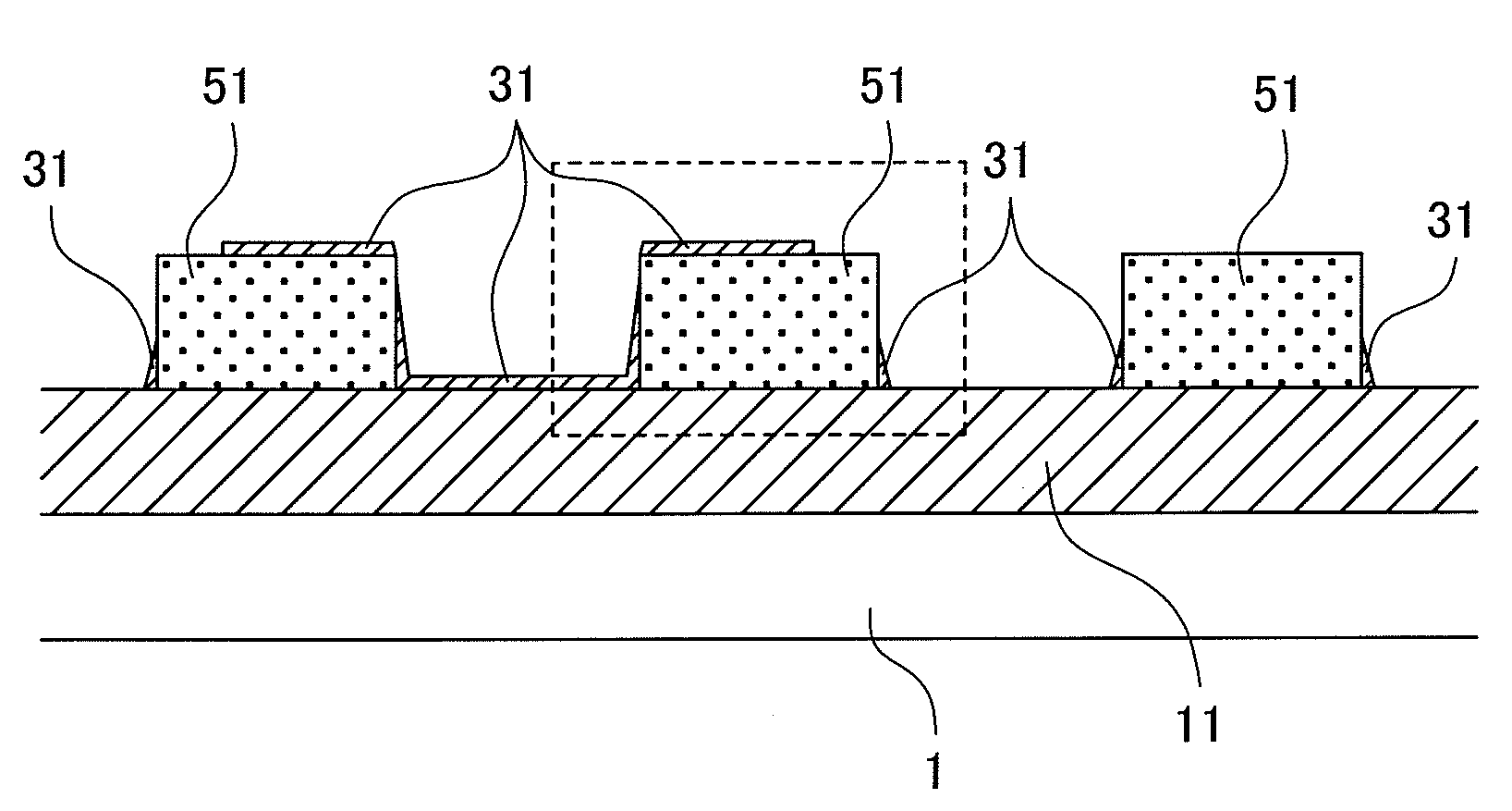
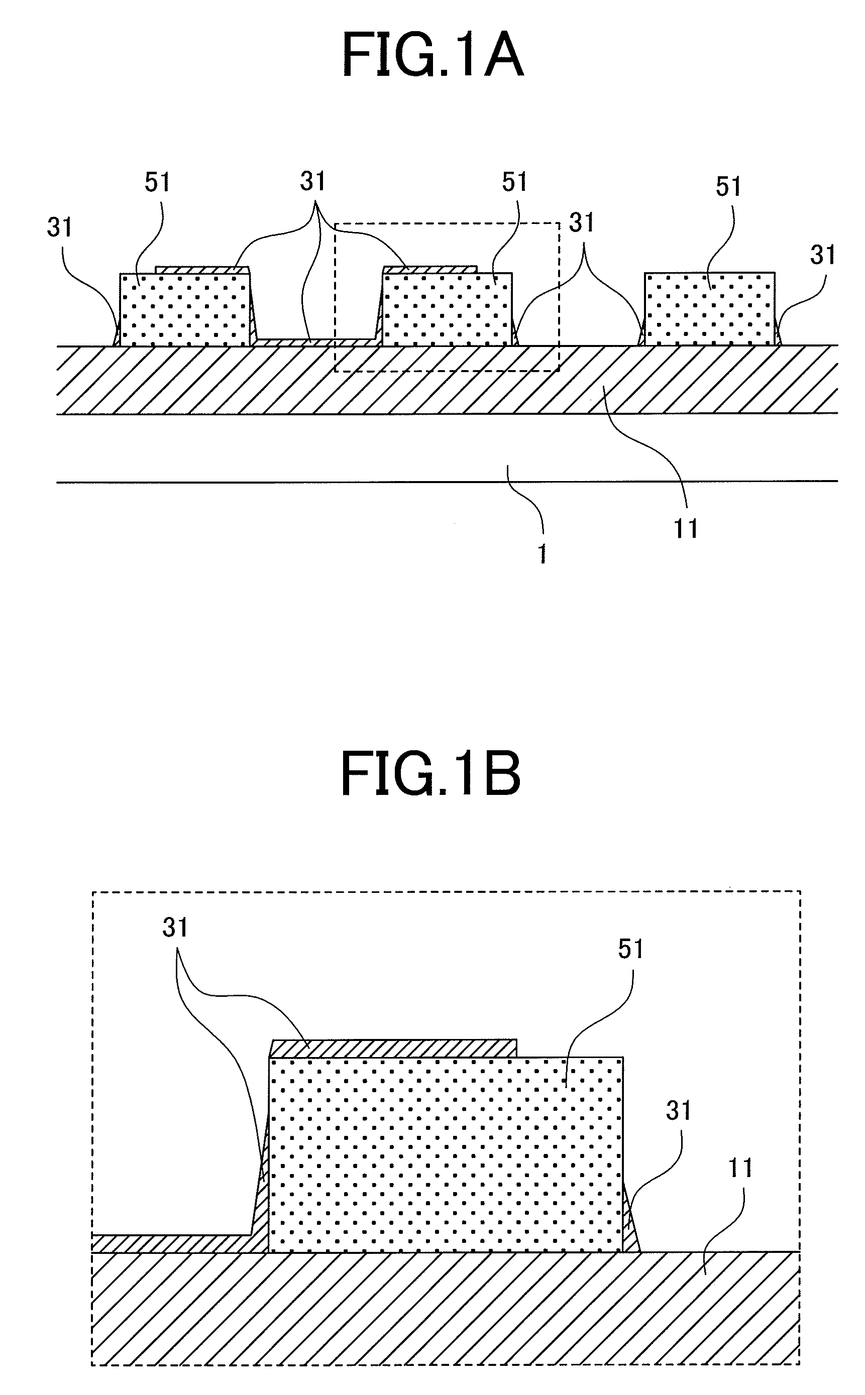
[0036]A first embodiment of a semiconductor device according to the present invention will be described below with reference to FIGS. 1A, 1B, 2, and 8A to 8D.
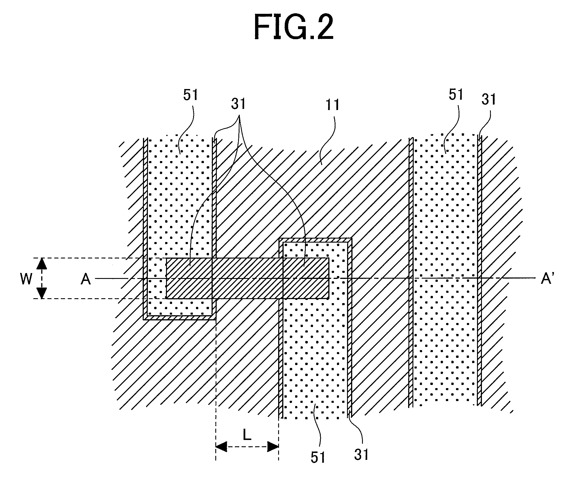
[0037]FIG. 2 schematically shows an example planar structure of thin metal film resistor elements according to the invention. As shown, thin metal film resistors are arranged to surround all wiring layers with one resistor element arranged to straddle between two separate wirings.
[0038]FIGS. 1A and 1B are cross-sectional views taken along line A-A′ in FIG. 2. All the cross-sectional views referred to in the present application are those taken along the same line. Thin metal films are formed in contact with lower side wall portions (lower peripheral portions) of wirings. Some thin metal film is formed over top portions of two wirings and a desired portion of insulation film in a manner of interconnecting the wirings. Thus, a thin metal film to be a resistor and wirings for electrode extraction are connected self-alignedly, so th...
second embodiment
[0043]A second embodiment of a semiconductor device according to the present invention will be described below with reference to FIGS. 3A, 3B, 4, and 9A to 9E.
[0044]FIG. 4 schematically shows an example planar structure of thin metal film resistor elements according to the present invention. As shown, thin metal film resistors are arranged to surround all wiring layers with one resistor element arranged to straddle between two separate wirings.
[0045]FIGS. 3A and 3B are cross-sectional views taken along line A-A′ in FIG. 4. A thin metal film 31 and a silicon nitride film 17 are laminated over a rough substrate surface. The silicon nitride film 17 is used as an etching mask for etching the thin metal film 31 so as to reduce changes in quality of the thin metal film of, for example, tantalum nitride (TaN) caused when the photoresist is removed by ashing. This method, compared with related art methods, makes it possible to more finely form resistors with higher precision.
[0046]FIGS. 9A ...
third embodiment
[0050]An embodiment of a method of manufacturing a semiconductor device according to the present invention will be described below with reference to FIG. 10. FIG. 10 shows an example of an integrated circuit including thin metal film resistors formed by the semiconductor device manufacturing method according to the present invention. As known from the example shown, the semiconductor device manufacturing method according to the present invention makes it possible to form high-precision resistors by a small number of processes even in cases where thin metal film resistors, bipolar transistors, CMOS transistors, MIM capacitors, and wirings are arranged in high density on a substrate. Furthermore, since a resistor layer can be combined with any wiring layer, it can be formed farther from the substrate than single-crystal silicon resistors and polycrystal silicon resistors. Hence, high-performance resistors with small parasitic capacitance can be easily realized.
[0051]As described above...
PUM
 Abstract
Description
Claims
Application Information
 - R&D
- Intellectual Property
- Life Sciences
- Materials
- Tech Scout
- Unparalleled Data Quality
- Higher Quality Content
- 60% Fewer Hallucinations
Browse by: Latest US Patents, China's latest patents, Technical Efficacy Thesaurus, Application Domain, Technology Topic, Popular Technical Reports.
© 2025 PatSnap. All rights reserved.Legal|Privacy policy|Modern Slavery Act Transparency Statement|Sitemap|About US| Contact US: help@patsnap.com