Photonic crystal sensors with intergrated fluid containment structure

a technology of intergrated fluid and photonic crystals, applied in the field of photonic band gap structures, can solve the problems of changing the photonic band gap, adding to the overall cost and complexity of fabrication of these devices, etc., and achieves the effects of enhancing the structural rigidity and flatness of the sensor, preventing leakage, and facilitating the handling of fluid samples

Active Publication Date: 2008-09-11
X BODY +1
View PDF10 Cites 45 Cited by
  • Summary
  • Abstract
  • Description
  • Claims
  • Application Information

AI Technical Summary

Benefits of technology

[0016]In these applications of the present disclosure, fluid containment structures, such as wells or fluid flow channels, are integrated with the sensor directly resulting in a monolithic, integral structure. The fluid contaiment structures can be designed to effectively convey the sample to the active area (periodic surface grating) of a photonic crystal. In some applications, the fluid containment structures further function in multichannel biosensor configurations to provide a fluid sample to a selected photonic crystal in a manner preventing the fluid sample spreading between adjacent sensors on the same substrate. Flow cells, such as microfluidic channels, are commonly used to provide a means for conveying a fluid sample through a narrow channel from a sample reservoir to the photonic crystal structure for analysis. Typical flow cell configurations employ an etched trench having an attached cover plate. These fluid containment and delivery systems must be precisely aligned to and effectively sealed against the photonic crystal active area so as to prevent leakage of sample. In other embodiments, the fluid containment structure is static, such as a cuvette aligned and bonded over the photonic crystal active area. In these embodiments, the photonic crystal sensor is provided as an internal surface of the cuvette. In multi-array configurations, for example, a large number of cuvettes each having an individually-addressed, independent photonic crystal sensors are provided in a microplate format, such as a 96, 384 or 1536 microarray format.
[0034]The manufacturing process may include replica molding process in which the transferring the pattern on the master grating basically forms a negative of the surface on the master template on the material. A periodic grating structure pattern having selected physical dimensions on the grating master is transferred to the material. Alternatively, the manufacturing method encompasses methods in which the pattern transfer is carried out using imprint lithography methods. Molding and imprinting fabrication methods of the present disclosure enable low cost, high throughput fabrication of photonic crystal arrays and sensing systems over very large areas (e.g., as large as 1 square foot at one time, upon a continuous roll of flexible substrate that may be thousands of meters in length). Methods of the present disclosure using replica molding for pattern transfer are beneficial because these methods do not require significant application of force to the external surface of the master template during pattern transfer, thereby avoiding damage to or distortion of grating structures in the master template relief pattern. This attribute of the present disclosure allows for repeat processing using a single master template and enhances pattern transfer fidelity. Use of polymer replica molding techniques are particularly beneficial as they can be carried out at room temperature and may be performed upon flexible and optically transparent substrates in a continuous roll-to-roll fashion.

Problems solved by technology

Given the submicron scale of features of the photonic crystal and micron or larger scale physical dimensions of the fluid containment structures, alignment and bonding steps in photonic crystal-based sensors present significant practical challenges, and thus add to the overall cost and complexity of fabrication of these devices.
Damage to such features can introduce unwanted defect structures to the photonic crystal that can strongly influence sensing capabilities and readout of the device.
In these embodiments, binding of analyte to a target material conjugated to the active surface of the photonic crystal causes a change in refractive index in a probe region, thereby affecting the coupling of electromagnetic radiation into the photonic crystal and resulting in a change in photonic band gap.

Method used


Image

  • Photonic crystal sensors with intergrated fluid containment structure
  • Photonic crystal sensors with intergrated fluid containment structure
  • Photonic crystal sensors with intergrated fluid containment structure

Examples


example 1

Single-Step Fabrication and Characterization of Photonic Crystal Biosensors with Polymer Microfluidic Channels

Introduction

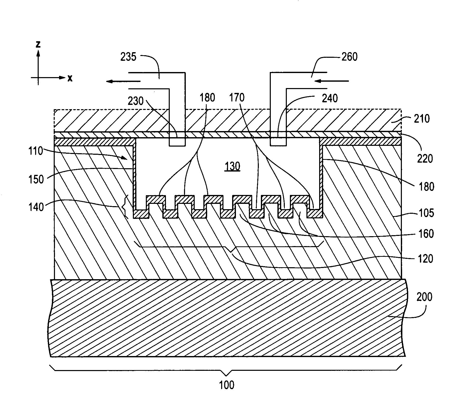
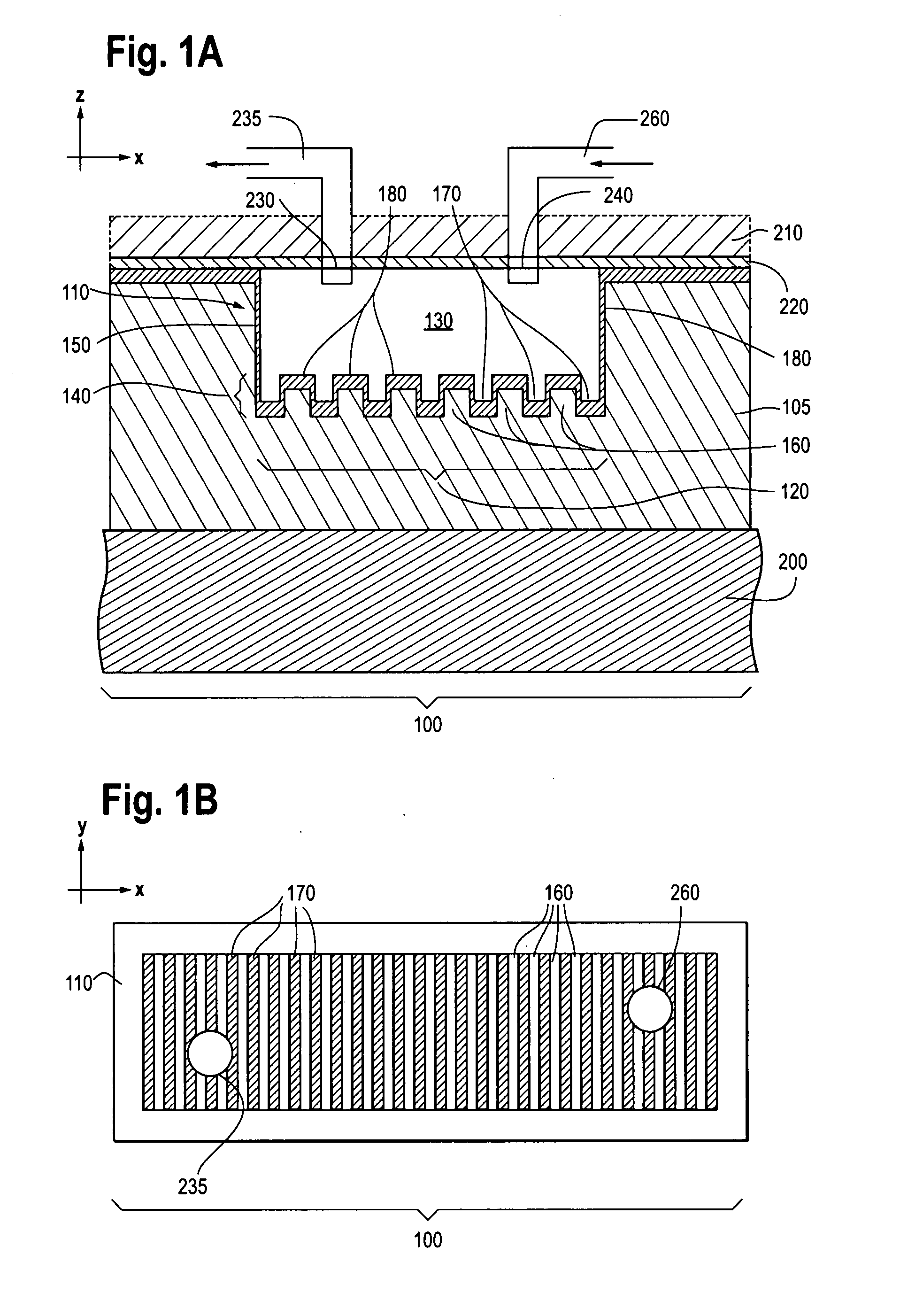
[0068]A method for simultaneously integrating label-free photonic crystal biosensor technology into microfluidic channels by a single step replica molding process is presented in this Example as one possible implementation of the disclosure.

[0069]By fabricating both the sub-micron features of the photonic crystal sensor structure and the >10 μm features of a flow channel network in one step at room temperature on a plastic substrate, the sensors are automatically self-aligned with the flow channels, and patterns of arbitrary shape may be produced. By measuring changes in the resonant peak reflected wavelength from the photonic crystal structure induced by changes in dielectric permittivity within an evanescent field region near its surface, detection of bulk refractive index changes in the fluid channel, or adsorption of biological material to the sensor surface ...

example 2

Photonic Crystal Sensors with Fluid Containment Structures Having a Microplate Configuration

[0108]Introduction

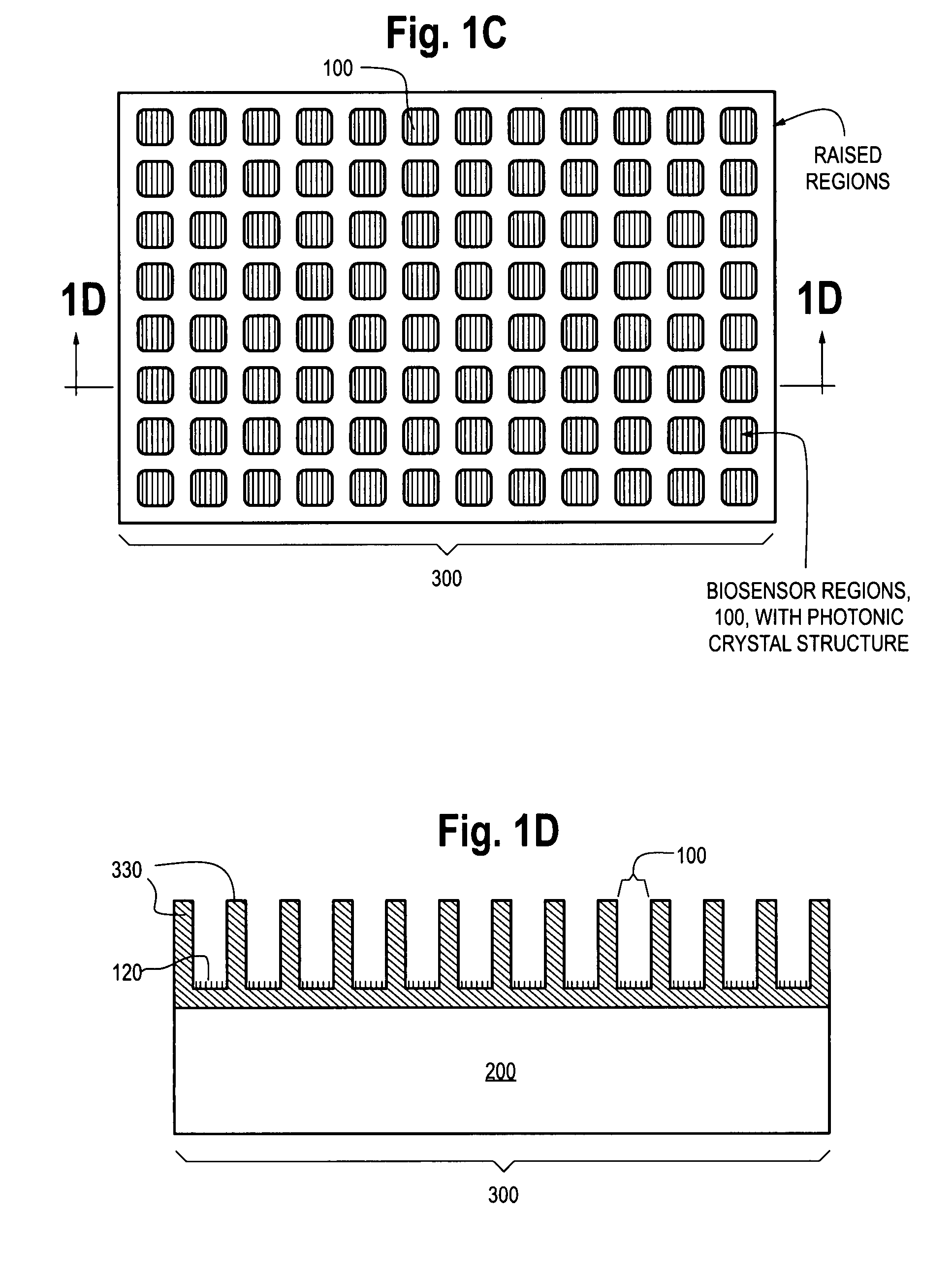
[0109]The present disclosure also contemplates microplate sensor systems comprising arrays of microwells, each having individually addressed photonic crystal sensors. Microplate sensor systems of this aspect of the present disclosure may further comprise integral micron scale fluid containment structures (channels) for introducing fluid samples containing analytes into selected microwells.

[0110]FIG. 9 is a schematic, top plan view of a microwell configuration 900 for a sensor system of this embodiment in the form of an array of 12×8 microwells 920. The sensor includes a fluid handling system 910 in the form of fluid channels 940 for delivery of fluid samples from ports 930 to the microwells 920. Each of the fluid channels 940 include photonic crystal sensors 950. The bottom surface of the microwells 920 include a photonic crystal sensor as shown the embodiment of FIG. 1A. Th...


PUM


Abstract

Photonic crystal (PC) sensors, and sensor arrays and sensing systems incorporating PC sensors are described which have integrated fluid containment and / or fluid handling structures. Sensors and sensing systems of the present disclosure are capable of high throughput sensing of analytes in fluid samples, bulk refractive index detection, and label-free detection of a range of molecules, including biomolecules and therapeutic candidates. The present disclosure also provides a commercially attractive fabrication platform for making photonic crystal sensors and systems wherein an integrated fluid containment structure and a photonic crystal structure are fabricated in a single molding or imprinting processing step amendable to high throughput processing.

Description

CROSS REFERENCE TO RELATED APPLICATIONS[0001]Pursuant to the provisions of 35 U.S.C. § 119 (e), this application claims priority to U.S. Provisional Application Ser. No. 60 / 865,093 filed Nov. 9, 2006, the content of which is incorporated by reference herein.STATEMENT REGARDING FEDERALLY SPONSORED RESEARCH OR DEVELOPMENT[0002]This invention was made, at least in part, with United States governmental support awarded by National Science Foundation under NSF DM1 03-28162. The United States Government has certain rights in this invention.BACKGROUND OF DISCLOSURE[0003]Photonic crystals, also commonly referred to as photonic bandgap structures, are periodic dielectric or metallic structures exhibiting a spatially periodic variation in refractive index that forbids propagation of certain frequencies of incident electromagnetic radiation. The photonic band gap of a photonic crystal refers to the range of frequencies of electromagnetic radiation for which propagation through the structure is ...

Claims


Application Information

Patent Timeline
Patent Type & Authority Applications(United States)
IPC IPC(8): G02B6/00
CPCB01L3/5027B01L3/5085B01L2300/0636G02B2006/1213B82Y20/00G01N21/253B01L2300/0654
Inventor CUNNINGHAM, BRIAN T.
Owner X BODY
Why Eureka
Try Eureka