Dielectric coatings for electrowetting applications

a technology of dielectric coatings and electrowetting, applied in the direction of variable capacitors, natural mineral layered products, instruments, etc., can solve the problems of limited current solutions using hydrocarbon or fluoropolymer insulating layers, and few materials combining both suitable dielectric and reliable hydrophobic properties within a broad thickness rang

Active Publication Date: 2008-09-18
INVENIOS FRANCE SAS
View PDF2 Cites 58 Cited by
  • Summary
  • Abstract
  • Description
  • Claims
  • Application Information

AI Technical Summary

Problems solved by technology

Current solutions using hydrocarbon or fluoropolymer insulating layers are limited due to their low dielectric strengths, necessitating thick insulating layers, typically on the order of 1 μm.
However, there are very few materials combining both suitable dielectric and reliable hydrophobic properties within a broad thickness range, especially when thickness is below one micrometer.

Method used

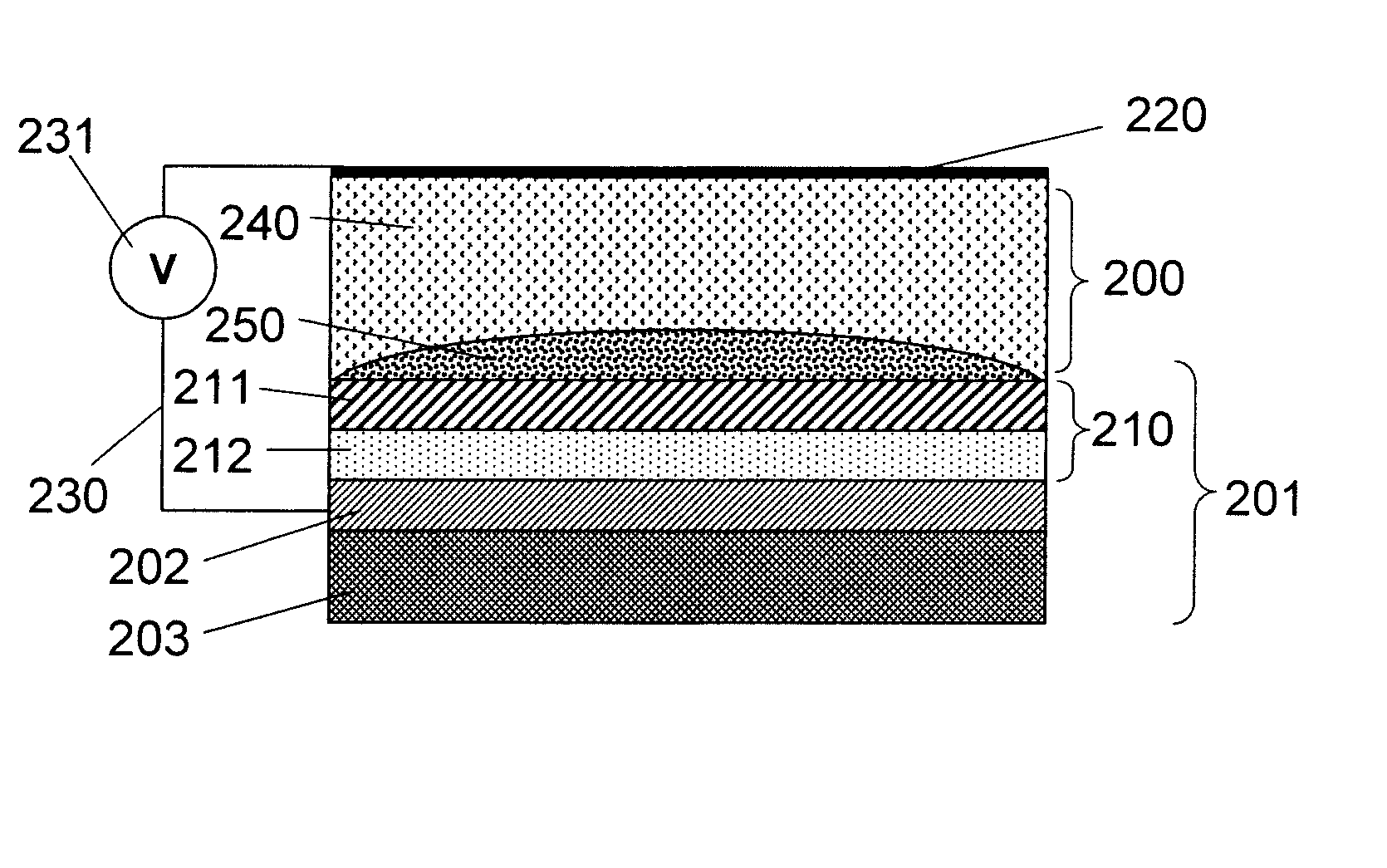
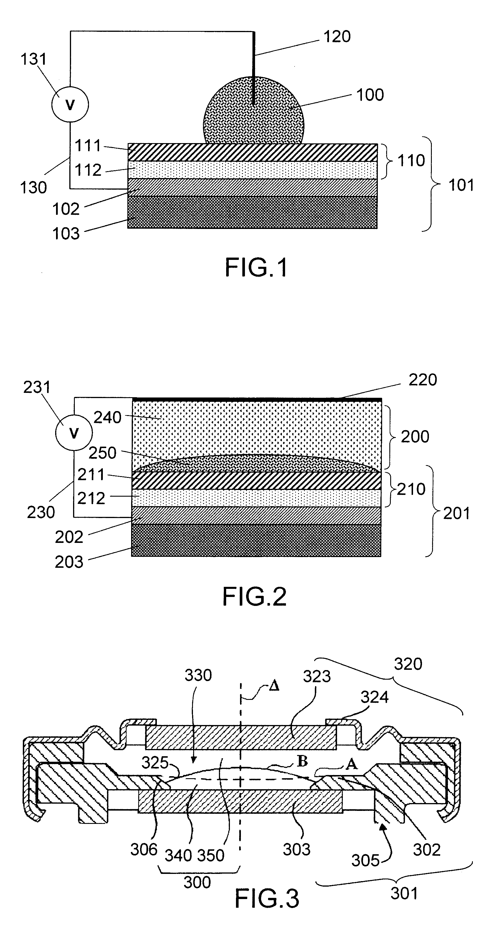
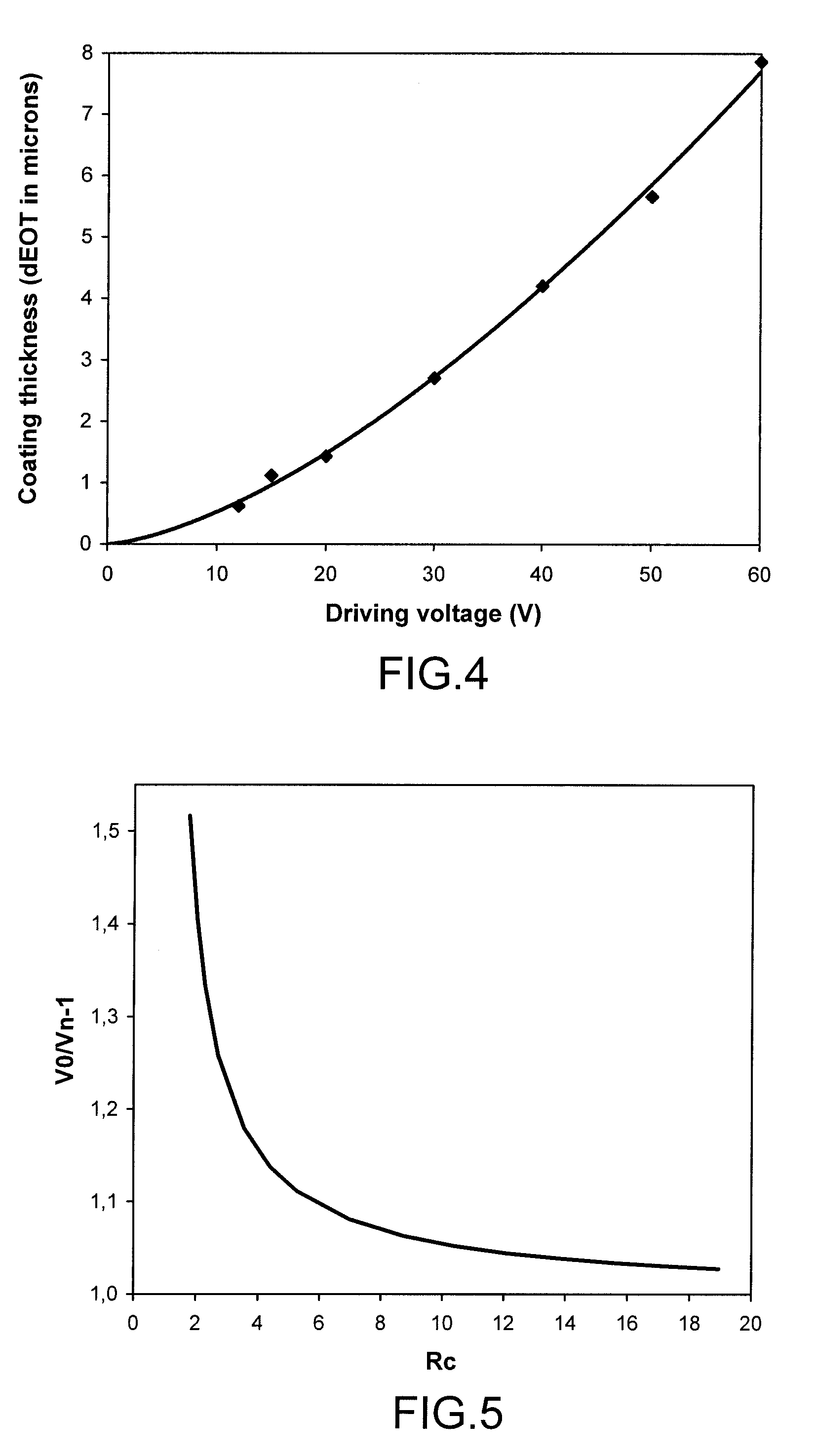

Image

  • Dielectric coatings for electrowetting applications
  • Dielectric coatings for electrowetting applications
  • Dielectric coatings for electrowetting applications

Examples


example 1

[0219]A two layer hydrophobic coating architecture composed of a silicon oxide layer and a subsequent hydrophobic layer was deposited onto nickel plated brass bodycone.

[0220]A 500 nm silicon oxide layer was deposited by PECVD of a SiH4 and N2O mixture. The substrate temperature was held at 200° C. during deposition. The dielectric constant and dielectric strength of the silicon oxide coating was 3.9 and 10 MV / cm, respectively. PECVD was conducted in a class 1 cleanroom to minimize defects in the coating.

[0221]A 90 nm organosiloxane coating was deposited by PECVD from tetramethyldisiloxane (TMDSO) at W / FM of 33 MJ / kg based on the process parameters including 500 W of applied power and 150 sccm TMDSO flowrate. The surface of the organosiloxane coating was characterized as hydrophobic based a reference liquid contact angle (RLCA) of 16.4±1.3 degrees, polar surface energy component of 1.4 mN / m and a dispersive surface energy component of 21.5 mN / m.

[0222]FIGS. 6, 8A and 8B show the exper...

example 2

[0225]A two layer hydrophobic coating architecture composed of a silicon oxide layer and a subsequent hydrophobic layer was deposited onto a P-type, boron doped, low resistivity (i.e. 0.01-0.02 ohm·cm) silicon wafer.

[0226]A 500 nm silicon oxide layer was deposited by PECVD of a SiH4 and N2O mixture. The substrate temperature was held at 400° C. during deposition. The dielectric constant and dielectric strength of the silicon oxide coating was 3.9 and 10 MV / cm, respectively. PECVD was conducted in a class 1 cleanroom to minimize defects in the coating.

[0227]A 90 nm organosiloxane coating was deposited by PECVD from tetramethyldisiloxane (TMDSO) at W / FM of 33 MJ / kg based on the process parameters listed in Table 2. The surface of the organosiloxane coating was characterized as hydrophobic based a reference liquid contact angle (RLCA) of 16.4±1.3 degrees, polar surface energy component of 1.4 mN / m and a dispersive surface energy component of 21.5 mN / m.

[0228]Coatings exhibited high diel...

example 3

[0229]A two layer hydrophobic coating architecture was deposited onto silicon wafers by the same process as in Example 2 using the same reagents. Coated wafers were annealed in a N2 purged vacuum oven for 1 hour at 400° C. The surface of the organosiloxane coating was characterized as hydrophobic based on reference liquid contact angle (RLCA) of 12.3±1.1 degrees.


PUM

PropertyMeasurementUnit
dielectric constantaaaaaaaaaa
thicknessaaaaaaaaaa
thicknessaaaaaaaaaa

Abstract

A dielectric coating is provided which has both a dielectric constant greater than 2.5 and a hydrophobic surface. The dielectric coating may be provided by plasma enhanced chemical vapor deposition (PECVD) of organosilane, organosiloxane, organosilazane, organometallic, and / or hydrocarbon precursors. Methods are also provided for altering the contact angle of a liquid in contact with the dielectric coating, e.g., for electrowetting applications.

Description

FIELD OF THE INVENTION [0001]The invention relates to improved dielectric coatings for devices which operate based on the electrowetting effect. In particular, the invention relates to dielectric coatings that function as both hydrophobic and dielectric layers.BACKGROUND OF THE INVENTION [0002]Electrowetting is a robust phenomenon in which the properties of both the insulating and the hydrophobic layers are critical. Substantial activities have been aimed at optimizing the properties of these layers in order to minimize the voltage required for water contact angle reduction and contact angle hysteresis. At the same time, the materials used should be chemically inert and stable in order to ensure reproducibility and a long lifetime.[0003]Such materials have been approached by using either an intrinsically hydrophobic insulator or by covering hydrophilic insulators with a thin hydrophobic top coating. Frequently, thin layers of amorphous fluoropolymers or hydrocarbon polymers (such as...

Claims


Application Information

Patent Timeline
Patent Type & Authority Applications(United States)
IPC IPC(8): G02B1/06B32B9/00H02N2/00
CPCG02B26/004G02B3/14Y10T428/31504Y10T428/31663
Inventor WEIKERT, CHRISTOPHER M.MARTIN, STEVEN J.MAILLARD, MATHIEULEGRAND, JULIEN
Owner INVENIOS FRANCE SAS
Why Eureka
Try Eureka