Ferroelectric capacitor and its manufacturing method

a technology of ferroelectric capacitors and manufacturing methods, applied in the direction of fixed capacitors, thin/thick film capacitors, instruments, etc., can solve the problems of poor ferroelectric characteristic, large leakage current of ferroelectric films, and inability to obtain good ferroelectric characteristics, so as to reduce leakage currents and reduce leakage currents , the effect of morphology roughness

Inactive Publication Date: 2008-09-18
SEIKO EPSON CORP
View PDF9 Cites 35 Cited by
  • Summary
  • Abstract
  • Description
  • Claims
  • Application Information

AI Technical Summary

Benefits of technology

[0020]According to the method for manufacturing a ferroelectric capacitor described above, the second ferroelectric layer composed of, for example, PZTN is formed on the first ferroelectric layer that is formed by a MOCVD method, and the third ferroelectric layer formed by a sol-gel method is further laminated on the second ferroelectric layer, whereby the ferroelectric film is formed. Therefore, as described above, even when roughness (morphology roughness) is formed on the surface of the first ferroelectric layer, the surface of the ferroelectric film can be made smooth by the third ferroelectric layer that is formed by a sol-gel method, whereby leakage current that may originate from morphology roughness can be reduced. Furthermore, the second ferroelectric layer composed of PZTN with few leakage current is formed between the first ferroelectric layer and the third ferroelectric layer, such that current leakage paths at the interface between the first ferroelectric layer formed by a MOCVD method and the third ferroelectric layer formed by a sol-gel method are embedded by the second ferroelectric layer, whereby leakage currents can be reduced.
[0021]Moreover, because the first ferroelectric layer is formed by a MOCVD method, the second ferroelectric layer and the third ferroelectric layer formed above the first ferroelectric layer have favorable crystal orientation, like the first ferroelectric layer, as the crystal orientation of their respective base layer is reflected in each of the layers, and thus the entire ferroelectric film can be provided with favorable crystal orientation, whereby the characteristic of ferroelectric capacitor having the ferroelectric film can be improved.

Problems solved by technology

This is because the conventional sputter method cannot form ferroelectric films with satisfactory crystal orientation characteristic, and good ferroelectric characteristic cannot be obtained, while ferroelectric films with good crystal orientation characteristic are desired.
However, the inventors have diligently studied ferroelectric films formed by the aforementioned MOCVD method, and discovered that ferroelectric capacitors obtained through forming a film of PZT by the MOCVD method to form a ferroelectric film had defects with considerable leakage current.
Although the cause of this considerable leakage current is not clear, it is believed that this may be caused by roughened morphology of the PZT film formed by the MOCVD method.
However, it was also found that, when the same PZT as that of the PZT film formed by the MOCVD method is used as the material for forming the second ferroelectric layer by the sol-gel method, the inversion charge (Qsw) became larger and the ferroelectric characteristic was improved, but paths of current leakage were formed at the interface between the PZT film formed by the MOCVD method and the PZT film formed by the sol-gel method, such that leakage currents were not sufficiently reduced.

Method used


Image

  • Ferroelectric capacitor and its manufacturing method
  • Ferroelectric capacitor and its manufacturing method
  • Ferroelectric capacitor and its manufacturing method

Examples


Embodiment Construction

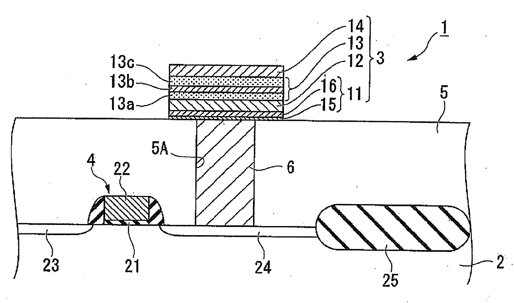
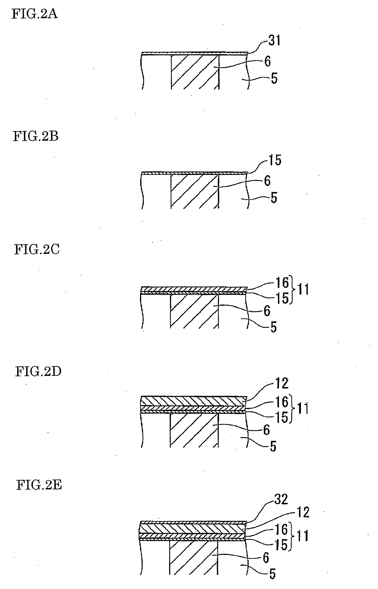
[0025]The invention is described below in detail. First, a ferroelectric capacitor in accordance with an embodiment of the invention is described with reference to the accompanying drawings. It is noted that, in each of the figures used for describing the invention, the scale of each of the members is appropriately changed to have a size that can be visually recognized.

[0026]FIG. 1 is a schematic cross-sectional view in enlargement of a ferroelectric memory device in a stacked structure that is equipped with a ferroelectric capacitor in accordance with an embodiment. Reference numeral 1 in FIG. 1 denotes the ferroelectric memory device, and reference numeral 3 denotes the ferroelectric capacitor.

[0027]The ferroelectric memory device 1 is equipped with a semiconductor substrate 2, the ferroelectric capacitor 3 formed on the semiconductor substrate 2, and a switching transistor (hereafter referred to as a transistor) 4 for the ferroelectric capacitor 3, as shown in FIG. 1.

[0028]The se...


PUM

PropertyMeasurementUnit
thicknessaaaaaaaaaa
thicknessaaaaaaaaaa
thicknessaaaaaaaaaa

Abstract

A ferroelectric capacitor includes: a ferroelectric film, and a lower electrode and an upper electrode interposing the ferroelectric film, wherein the ferroelectric film includes a first ferroelectric layer of ferroelectric material having a perovskite type crystal structure expressed by a general formula ABO3 formed by a metal organic chemical vapor deposition method, a second ferroelectric layer of ferroelectric material in which a part of B site element in ferroelectric material having a perovskite type crystal structure expressed by a general formula ABO3 is replaced with Nb, and a third ferroelectric layer of ferroelectric material having a perovskite type crystal structure expressed by a general formula ABO3 formed by a sol-gel method, which are sequentially laminated from the side of the lower electrode.

Description

[0001]The entire disclosure of Japanese Patent Application No. 2007-064596, filed Mar. 14, 2007 is expressly incorporated by reference herein.BACKGROUND[0002]1. Technical Field[0003]The present invention relates to ferroelectric capacitors and methods for manufacturing the same.[0004]2. Related Art[0005]Ferroelectric memory devices (FeRAM) are nonvolatile memory devices capable of low voltage and high-speed operation, using spontaneous polarization of the ferroelectric material, and their memory cells can be each formed from one transistor and one capacitor (1T / 1C). Accordingly, ferroelectric memory devices can achieve integration at the same level of that of DRAM, and are therefore expected as large-capacity nonvolatile memories.[0006]As the material for forming the ferroelectric film that composes the ferroelectric capacitor, in other words, as the ferroelectric material, a material having a perovskite type crystal structure expressed by a general formula ABO3, more specifically, ...

Claims


Application Information

Patent Timeline
Patent Type & Authority Applications(United States)
IPC IPC(8): G11C11/22
CPCH01G4/085H01G4/1218H01G4/33H01L28/57H01L27/11502H01L27/11507H01L21/31691H01L21/02197H01L21/02266H01L21/02282H01L21/022H01L21/02271H10B53/30H10B53/00
Inventor NAWANO, MASAHISA
Owner SEIKO EPSON CORP
Why Eureka
Try Eureka