Synchronous imaging using segmented illumination

a segmented illumination and imaging system technology, applied in the field of photodetectors, can solve the problems of less readily available sensors capable of detecting such wavelengths, generally more expensive than, and lower cost of these devices, so as to improve improve the sensitivity of an image sensor, and improve the effect of the performance of an active illumination imaging system

Active Publication Date: 2008-10-09
APTIV TECH LTD
View PDF11 Cites 47 Cited by
  • Summary
  • Abstract
  • Description
  • Claims
  • Application Information

AI Technical Summary

Benefits of technology

[0011]A method and system for an actively illuminated imaging system is provided. The present invention improves the performance of an actively illuminating imaging system by synchronizing the illumination of a specific scene portion with a photosensitive period of a portion of an imaging array that is at the moment in time capable of sensing the specific scene portion. In an embodiment, the present invention spatially varies an irradiance pattern allowing a more uniform distribution of light by redistributing intensity away from the center of a field to the periphery of the field. The sensitivity of an image sensor is maximized, while simultaneously minimizing the amount of light that must be supplied to illuminate a scene. Therefore, a wider margin of safety is provided between image sensing system operating conditions and eye safety limiting conditions. Further, because the distribution of emitted light is widened, being emitted from multiple locations within the illumination system, the intensity of light at any physical location in the path of the light is reduced, thus further improving the eye safety margin. Electrical power reductions and heat reductions is achieved by limiting the generation of light that cannot currently be detected by the imaging portion of the system. Alternatively, higher total illumination of a scene, at the same power levels of contemporary systems, is achieved. Improvement in signal to noise ratio is also provided given the same illumination power as contemporary systems.

Problems solved by technology

The pervasive nature of silicon based integrated circuits, and consequently that of silicon based photodetectors and silicon base imager chips, makes the resulting cost of these devices lower than the cost of devices fabricated using other materials and technologies, that might offer other ranges of spectral sensitivity.
Generally, however, sensors capable of detecting such wavelengths are less readily available, and generally more expensive than those that detect light in various portions of the infrared wavelength regime.
Additionally, wavelengths shorter than approximately 420 nm become increasingly hazardous to both the human eye and other portions of the human body as the wavelength is reduced further into the ultraviolet regime.
Consequently, such short wavelength light is generally not as convenient to use for imager and detector systems.
In addition, silicon based devices are generally not sensitive to wavelengths significantly lower than approximately 350 nm, which presents another impediment to the use of such short wavelengths for imaging and detection applications, as compared to systems operating at near-infrared wavelengths.
Eye safety issues limit the maximum irradiance of illumination sources for actively illuminated non-visible imaging applications.
These eye-safety limitations represent a major challenge for sensing applications in which ambient lighting varies by a large amount, since an actively illuminated sensing system must be capable of essentially overpowering ambient lighting, such as sun light.
However, if either the detector or objects in the scene are moving, additional constraints are placed upon the amount of time available for charge collection, which may limit the detector sensitivity.
On the other hand, as detector areas increase, so does cost.
Consequently, increasing sensitivity by arbitrary increases in detector area generally is not acceptable.
If the detectors do not all start and stop collecting light at the same time, then objects in the image could be distorted due to relative motion of the imaging array and the scene being imaged.
Illuminating the scene during these periods essentially wastes that portion of the illumination, since it cannot be detected.
This requires a complicated pixel structure, entailing more transistors per pixel.
Consequently, the pixels are larger for a given photocollection area, and the imager array will cost more with lower sensitivity.

Method used


Image

  • Synchronous imaging using segmented illumination
  • Synchronous imaging using segmented illumination
  • Synchronous imaging using segmented illumination

Examples


Embodiment Construction

[0034]Exemplary embodiments are described with reference to specific configurations. Those of ordinary skill in the art will appreciate that various changes and modifications can be made while remaining within the scope of the appended claims. Additionally, well-known elements, devices, components, methods, process steps and the like may not be set forth in detail in order to avoid obscuring the invention. Further, unless indicated to the contrary, the numerical values set forth in the following specification and claims are approximations that may vary depending upon the desired characteristics sought to be obtained by the present invention.

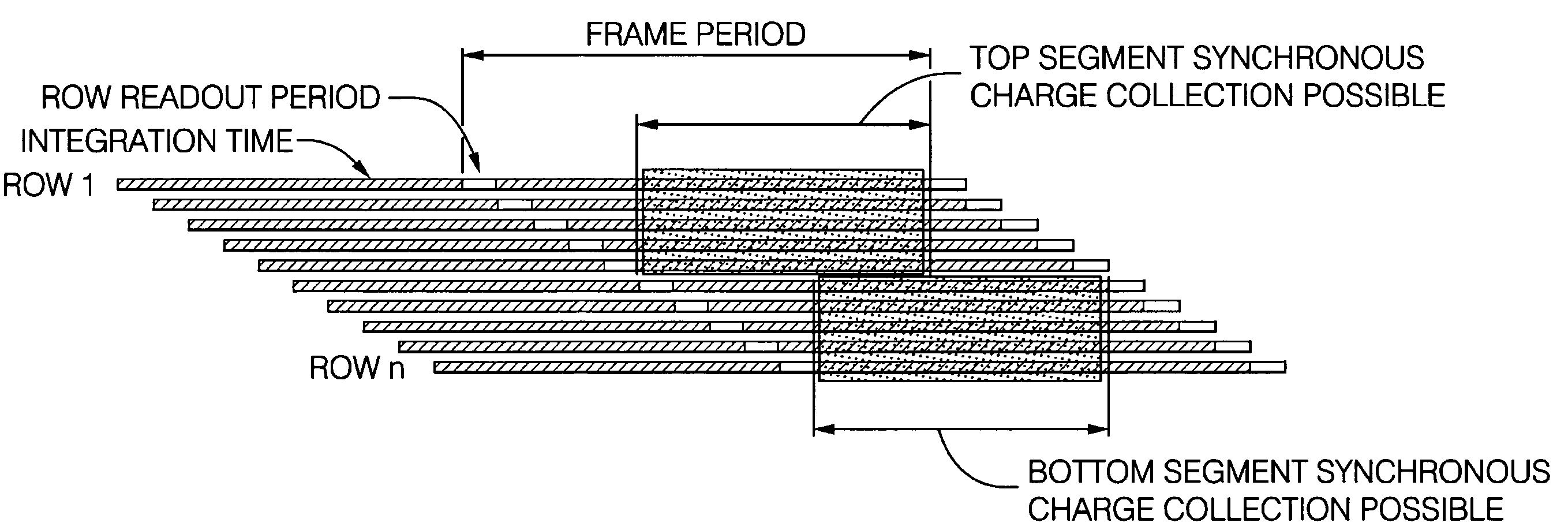
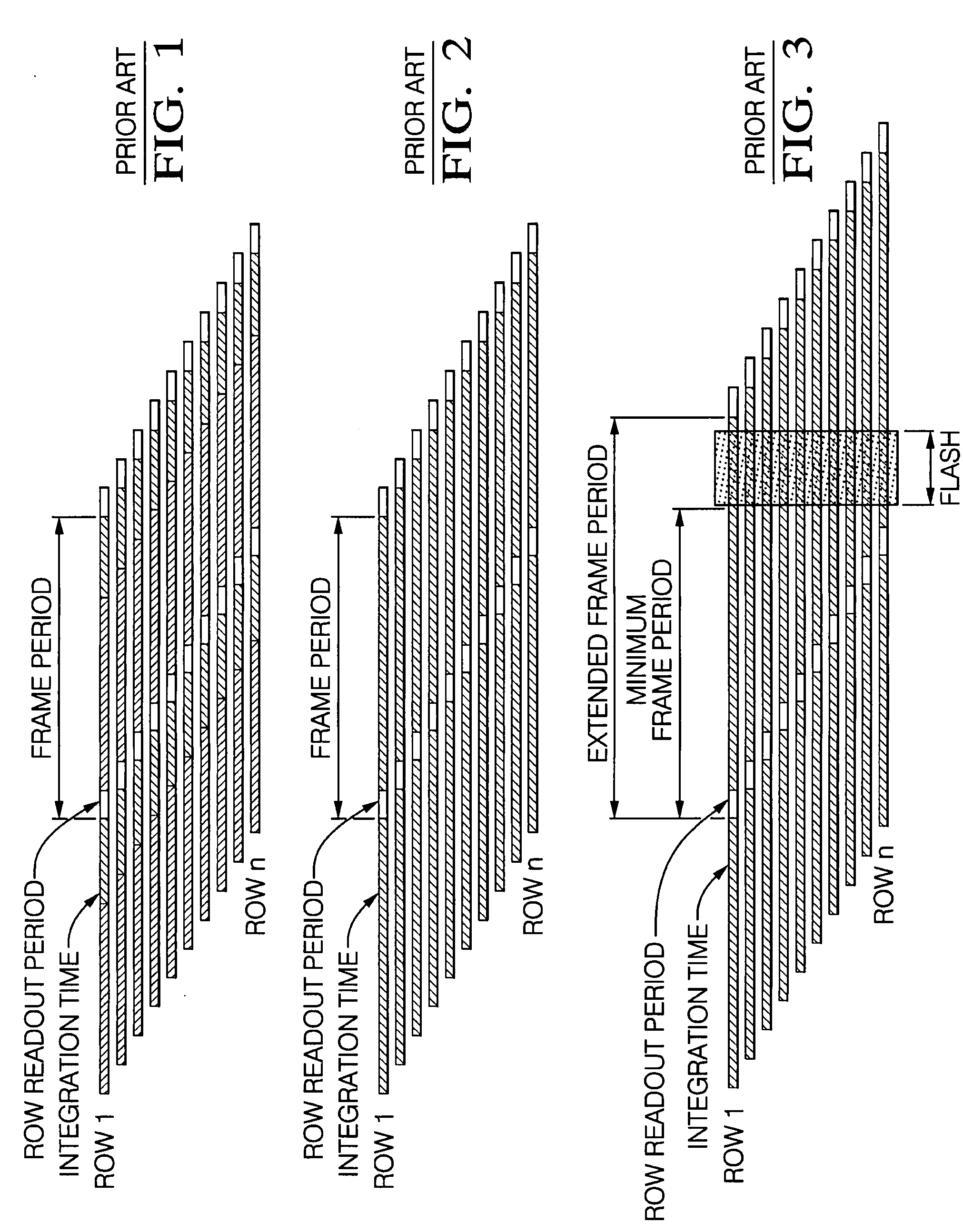
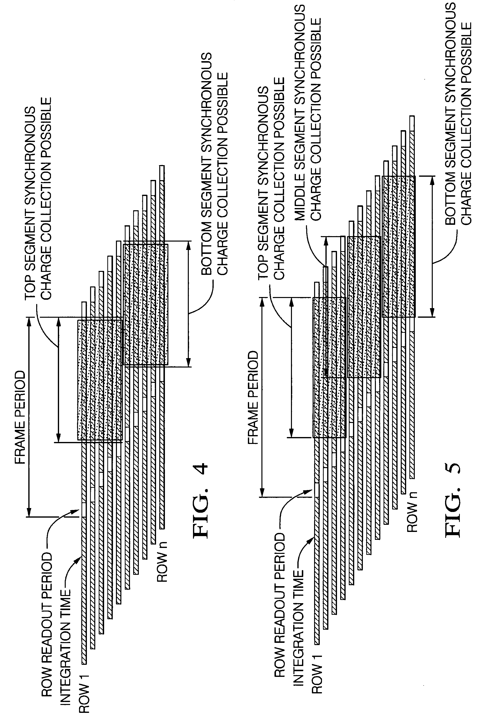
[0035]A method and system are described herein for an actively illuminated imaging system. The present invention improves the illumination of a scene by synchronizing an illumination of a segment or portion of a scene when an imager is actively collecting photogenerated charge from that portion of the scene. The present invention can spatially va...


PUM


Abstract

In an actively illuminated imaging system, illumination of a segmented scene is synchronized with an image sensing period. A scene is segmented into a plurality of scene portions utilizing a segmented lens. In an aspect, a first scene portion is illuminated when an imager is actively collecting photogenerated charge from the first scene portion, and a second scene portion is illuminated when an imager is actively collecting photogenerated charge from the second scene portion. The sensitivity of an image sensor is maximized, while simultaneously minimizing the amount of light that must be supplied to illuminate a scene. An irradiance pattern is varied allowing a more uniform distribution of light. Bands of varying wavelength, polarization, and light intensity may be variously applied to illuminate individual scene segments, as needed to enhance an identification of an object in the scene. The present invention is particularly useful with high frame rate imaging systems.

Description

FIELD OF THE INVENTION[0001]The invention relates generally to a photodetector, and more particularly to synchronizing the illumination of a segmented scene with an image sensing period, in an actively illuminated imaging system.BACKGROUND OF THE INVENTION[0002]Numerous imaging applications require integrated or active illumination to augment ambient lighting and / or to ensure constant scene illumination irrespective of other illumination sources. This is especially true with imagers having higher frame rates. In many cases, it is necessary or desirable for such illumination sources to be non-visible to the human eye, but detectible by an image sensing device.[0003]A generally employed technique for providing non-visible illumination, as defined by the ability to be detected by the human visual system, is to use wavelengths that are longer than the human eye can detect. Generally, these are referred to as infrared wavelengths. Infrared light comprises light with wavelengths in excess...

Claims


Application Information

Patent Timeline
Patent Type & Authority Applications(United States)
IPC IPC(8): H01L27/00
CPCG03B15/05H04N5/2256H04N5/2354H04N5/3532G03B2215/0567G03B2215/0592H04N23/56H04N23/74H04N25/531
Inventor TROXELL, JOHN R.TAYLOR, RONALD M.REGE, SIDDHARTH S.
Owner APTIV TECH LTD
Why Eureka
Try Eureka