Charge trap flash memory device and memory card and system including the same

a technology of flash memory and charge trap, which is applied in the field of flash memory, can solve the problems of high operating voltage and low program speed of sonos memory devices, insufficient charge retention duration in vertical or horizontal directions, and high operating voltage of silicon oxide layers, etc., and achieve the effect of improving charge storage capacity

Active Publication Date: 2008-10-09
SAMSUNG ELECTRONICS CO LTD
View PDF4 Cites 45 Cited by
  • Summary
  • Abstract
  • Description
  • Claims
  • Application Information

AI Technical Summary

Benefits of technology

[0018]In accordance with aspects of the present invention, there is provided a charge trap flash memory device having a structure that can prevent charges stored in a charge trap layer from being lost and can improve a charge storage capacity.
[0019]Also in accordance with aspects of the present invention, there is provided a method that can be used to simply and easily manufacture the charge trap flash memory device having a structure that can prevent charges stored in a charge trap layer from being lost and can improve a charge storage capacity.

Problems solved by technology

However, in the SONOS memory device, dielectric constants of a silicon nitride layer and silicon oxide layers are low, and an electron trap site density is not sufficient in the silicon nitride layer and, as such, the SONOS memory device has a high operating voltage and a low program speed.
Also, charge retention duration in a vertical or horizontal direction is not sufficient.
On the other hand, the TANOS structure has a high erasing voltage and poor retention characteristics.
An erasing voltage and reliability can be improved in the NAN structure, but there is a disadvantage in that it has a low program voltage and high threshold voltage disturbance characteristics.

Method used


Image

  • Charge trap flash memory device and memory card and system including the same
  • Charge trap flash memory device and memory card and system including the same
  • Charge trap flash memory device and memory card and system including the same

Examples


Embodiment Construction

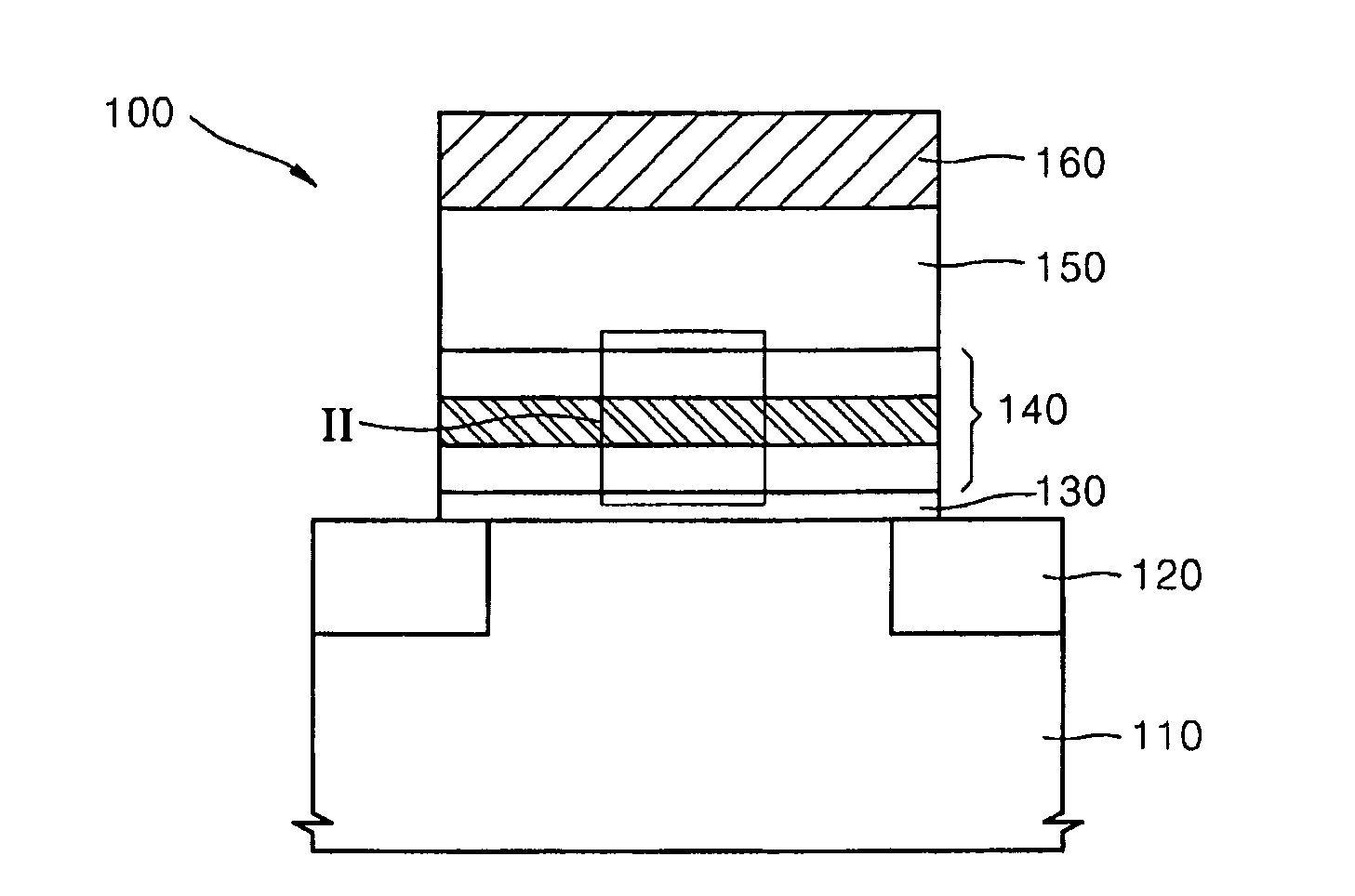
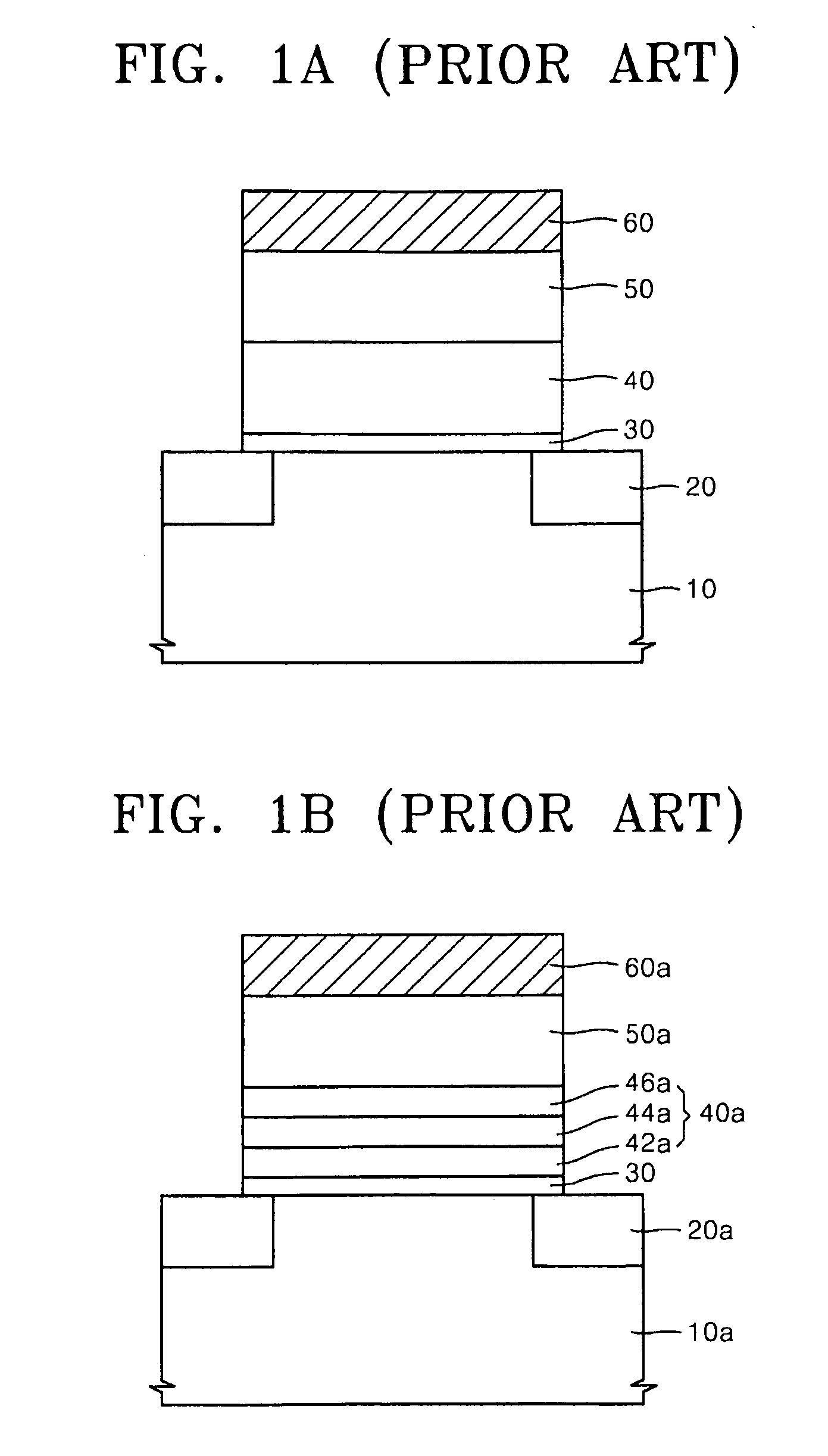
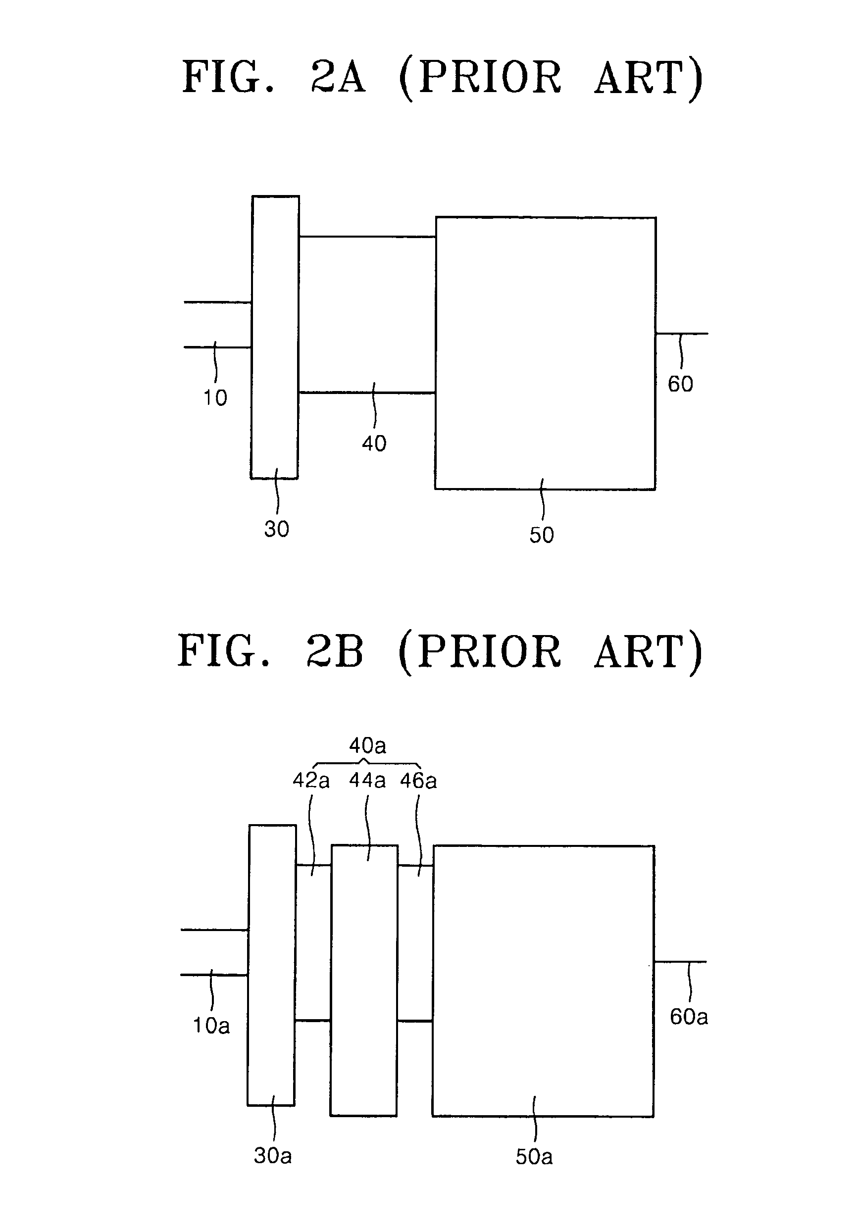
[0055]Hereinafter, aspects of the present invention will be described by explaining illustrative embodiments in accordance therewith, with reference to the attached drawings. While describing these embodiments, detailed descriptions of well-known items, functions, or configurations are typically omitted for conciseness.

[0056]The invention can, however, be embodied in many different forms and should not be construed as being limited to the embodiments set forth herein; rather, these embodiments are provided so that this disclosure will be thorough and complete, and will fully convey the concept of the invention to those skilled in the art. It will also be understood that when a layer is referred to as being “on” another layer or substrate, it can be directly on the other layer or substrate, or intervening elements can also be present. In the drawings, the thicknesses sizes of layers and regions are exaggerated for clarity. Like reference numerals in the drawings denote like elements,...


PUM


Abstract

A charge trap flash memory device and method of making same are provided. The device includes: a tunnel insulating layer, a charge trap layer; a blocking insulating layer; and a gate electrode sequentially formed on a substrate. The charge trap layer includes: plural trap layers comprising a first material having a first band gap energy level; spaced apart nanodots, each nanodot being at least partially surrounded by at least one of the trap layers, wherein the nanodots comprise a second material having a second band gap energy level that is lower than the first band gap energy level; and an intermediate blocking layer comprising a third material having a third band gap energy level that is higher than the first band gap energy level, formed between at least two of the trap layers. This structure prevents loss of charges from the charge trap layer and improves charge storage capacity.

Description

CROSS-REFERENCE TO RELATED PATENT APPLICATION[0001]This application claims priority to Korean Patent Application No. 10-2007-0032939, filed on Apr. 3, 2007, in the Korean Intellectual Property Office, the disclosure of which is incorporated herein in its entirety by reference.BACKGROUND OF THE INVENTION[0002]1. Field of the Invention[0003]The present invention relates to a flash memory, and more particularly, to a charge trap flash (CTF) memory device and memory card, and system including the same.[0004]2. Description of the Related Art[0005]In general, non-volatile memory devices are semiconductor memory devices in which data stored therein is not erased even if power supply thereto is stopped. Since the non-volatile memory devices have a high data storage capacity, they have been widely employed in mobile communication systems, memory cards, etc.[0006]In the case of a NAND type flash semiconductor memory device, which is an example of a high capacity non-volatile semiconductor mem...

Claims


Application Information

Patent Timeline
Patent Type & Authority Applications(United States)
IPC IPC(8): H01L29/792
CPCB82Y10/00H01L21/28273H01L29/42332H01L29/7881H01L29/40114H01L29/40117
Inventor HUO, ZONG-LIANGYEO, IN-SEOKLIM, SEUNG-HYUNJOO, KYONG-HEEYANG, JUN-KYU
Owner SAMSUNG ELECTRONICS CO LTD
Why Eureka
Try Eureka