
Photoimprintable Low Dielectric Constant Material and Method for Making and Using Same

a dielectric constant, low-dielectric technology, applied in the direction of photomechanical equipment, circuit masks, instruments, etc., can solve the problems of time-consuming, expensive, and inability to meet the requirements of the device, and achieve the effect of reducing the cost of production and production

Inactive Publication Date: 2008-10-30
VERSUM MATERIALS US LLC
View PDF30 Cites 10 Cited by
  • Summary
  • Abstract
  • Description
  • Claims
  • Application Information

AI Technical Summary

Problems solved by technology

These patterning steps are time consuming, expensive, and could potentially introduce defects into the device.

Method used


Image

  • Photoimprintable Low Dielectric Constant Material and Method for Making and Using Same
  • Photoimprintable Low Dielectric Constant Material and Method for Making and Using Same
  • Photoimprintable Low Dielectric Constant Material and Method for Making and Using Same

Examples


example 1

Low-Solvent Photodefinable Film Containing PAG

[0062]In Example 1, a film-forming composition was prepared containing the following: 18.0 grams of MTES as the silica source, 2.0 g of ethanol, 4.4 grams of the PAG (Bis(4-tert-butylphenyl)iodonium) triflate, and 6 grams of water. The composition was aged for 3 days and then the composition was partially polymerized by heating the composition to a temperature of 50° C. under vacuum to remove excess water and ethanol present from silicate hydrolysis. The viscosity of the aged and partially polymerized material was measured. The viscosity of the aged material was an average of 69cP when measured using a Brookfield viscometer at 25° C. at 100 rpm and torque of 2.8%. The resultant composition is suitable, for example, for spin casting onto substrate or ink jet printing onto substrates.

example 2

Low-Solvent Photodefinable Film Containing PAG

[0063]In Example 2, a film-forming composition was prepared containing the following: 18.0 grams of MTES as the silica source, 2.7 g of ethanol, 4.4 grams of the PAG (Bis(4-tert-butylphenyl)iodonium) triflate, and 6 grams of water. The composition was aged for 6 days. Thereafter, the composition was partially polymerized by heating the composition to a temperature of 50° C. under vacuum to remove excess water and ethanol present from silicate hydrolysis. The viscosity of the aged and partially polymerized material was an average of 69 cP when tested at the same conditions as in Example 1. This solution was diluted with propylene glycol propyl ether (PGPE) and the solution spun onto a low resistivity silicon substrate, wherein the material was exposed to broad band UV radiation for 10 sec. The broad band ultraviolet light source referred to herein is manufactured by Fusion Systems using a “D” bulb, for 5 second. The films were baked at 90...

example 3

Low-Solvent Photodefinable Film Containing PAG and Porogen

[0066]In Example 3, a film-forming composition was prepared containing the following: 18.0 grams of MTES as the silica source, 2.0 grams of ethanol, 0.42 grams of the PAG (Bis(4-tert-butylphenyl)iodonium) triflate, 4.0 grams of Triton X-114 and 6 grams of water. The composition was aged 6 days. Thereafter, the composition was partially polymerized to remove excess water and ethanol present from silicate hydrolysis. Using a Model DVII Brookfield viscometer at 25° C. and a # 34 spindle, a viscosity of 76-90 cP was measured at 50 rpm using a torque of 0.7%. This solution was diluted with PGPE and the solution spun onto a low resistivity silicon substrate, wherein the material was exposed to broad band UV radiation using the source described above in Example 2 for 10 seconds. The films were baked at 90° C. for 90 seconds, with a second bake performed at 180° C. for 90 seconds and a third bake was performed at 250° C. for 90 secon...


PUM

PropertyMeasurementUnit
dielectric constantaaaaaaaaaa
molar ratioaaaaaaaaaa
viscosityaaaaaaaaaa

Abstract

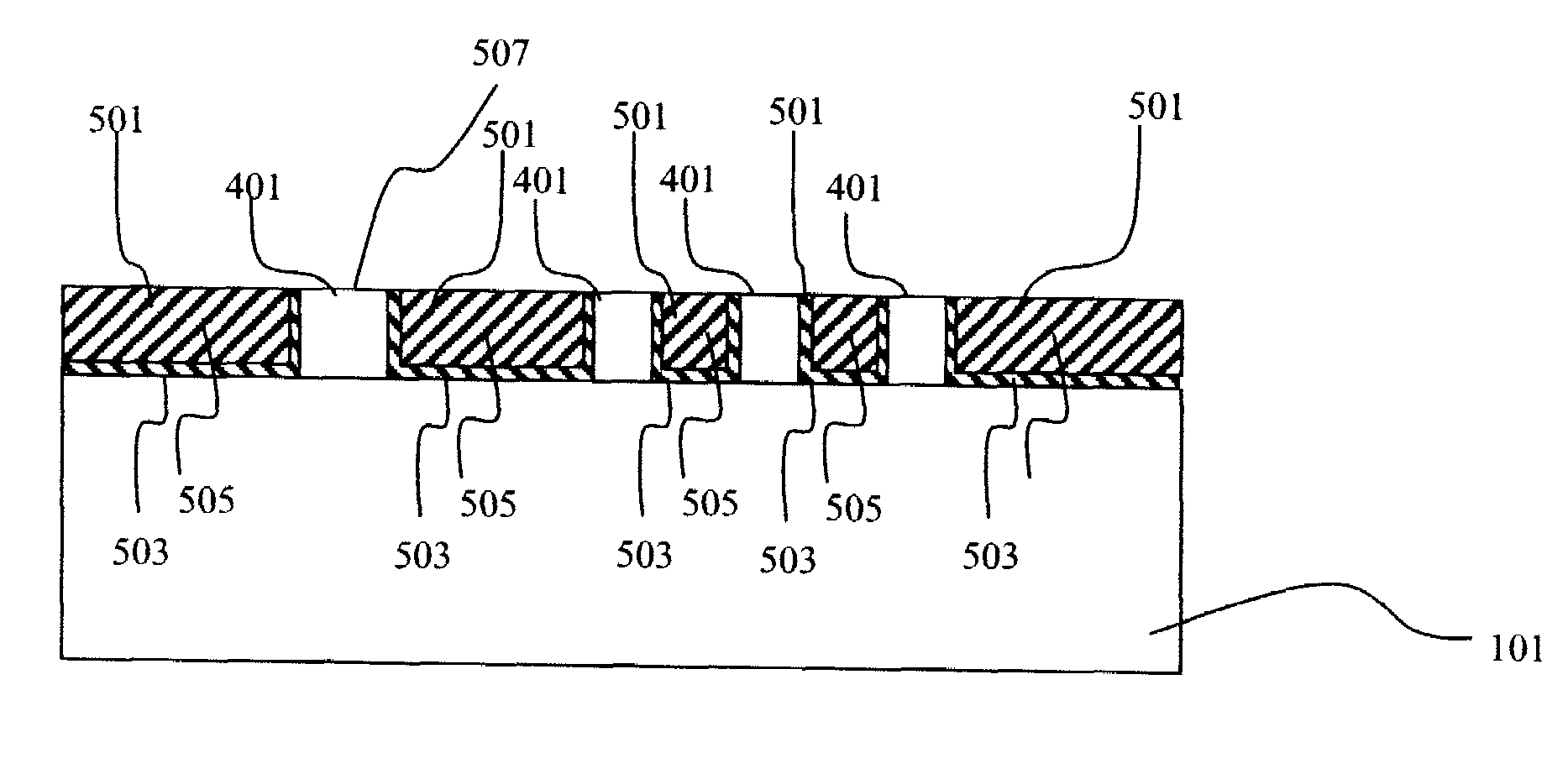
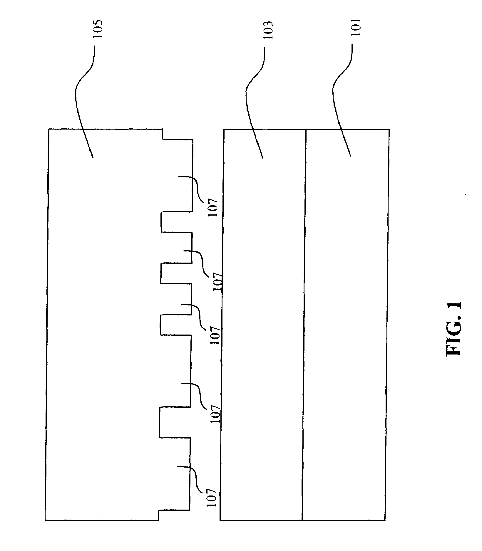
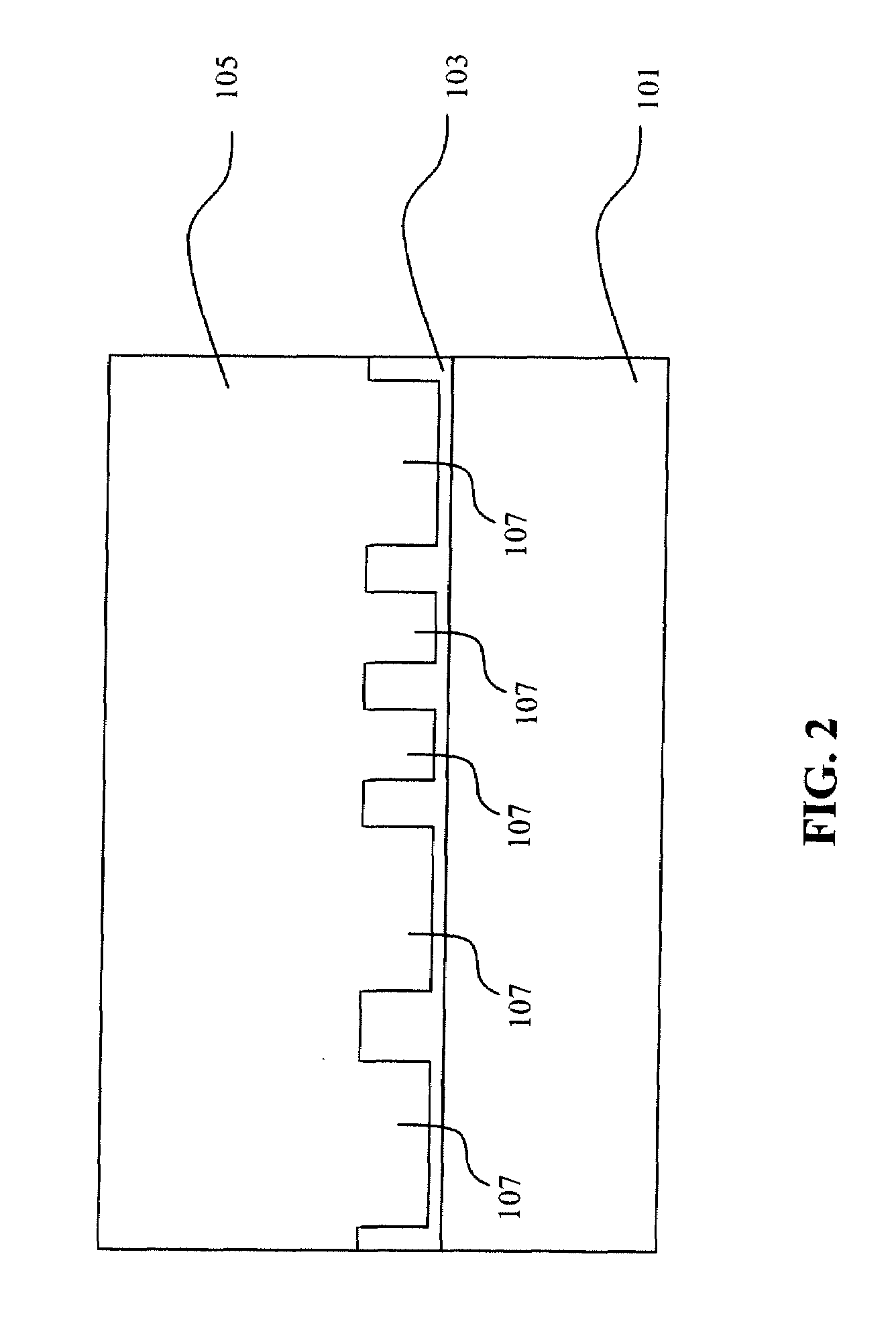
A process for preparing a photoimprinted film, a composition for forming a photoimprinted film and a photoimprinted film comprising a dielectric constant of less than about 3.5. The method includes providing a material film having a composition including at least one silica source capable of being sol-gel processed, at least one photoactive compound and at least one solvent; and water. The composition contains less than about 0.1% by weight of an added acid. A mold having mold features is provided. The mold is positioned in sufficient contact with the material film to allow the material to contact at least a portion of the mold features. The material film is then exposed to a radiation source and the film is cured to form a solidified material film. The mold is separated from the solidified material, wherein the material includes film features corresponding to the mold features.

Description

CROSS-REFERENCE TO RELATED APPLICATIONS[0001]This application is related to U.S. patent application Ser. No. 11 / 341,334 filed Jan. 27, 2006, which is hereby incorporated by reference in its entirety.BACKGROUND OF THE INVENTION[0002]The present invention is directed to photoimprinting, compositions for photoimprinting and photoimprinted products and devices utilizing photoimprinted materials.[0003]There is a continuing desire in the microelectronics industry to increase the circuit density in multilevel integrated circuit devices such as memory and logic chips in order to improve the operating speed and reduce power consumption. Current fabrication routes, such as conventional photolithography, for forming integrated circuits and similar electrical devices include numerous processing steps to place metal features in a specific location within a low dielectric constant film. These steps may include the deposition of a low dielectric film, deposition of a photoresist, creating a patter...

Claims


Application Information

Patent Timeline
Patent Type & Authority Applications(United States)
IPC IPC(8): H05K1/00B29C35/04
CPCB82Y10/00B82Y40/00G03F7/0002H05K3/0073H05K3/107H05K2203/0108
Inventor MARKLEY, THOMAS JOHNWEIGEL, SCOTT JEFFREYKRETZ, CHRISTINE PECK
Owner VERSUM MATERIALS US LLC
Learn More