Ultra-Sensitive Optical Detector With High Time Resolution

a detector and ultra-sensitive technology, applied in the field of ultra-sensitive optical detectors with large time resolution, can solve the problems of affecting reducing the detection efficiency of a single detector, so as to achieve the effect of reducing the noise, reducing the noise, and high values

Inactive Publication Date: 2008-11-06
COMMISSARIAT A LENERGIE ATOMIQUE ET AUX ENERGIES ALTERNATIVES
View PDF12 Cites 64 Cited by
  • Summary
  • Abstract
  • Description
  • Claims
  • Application Information

AI Technical Summary

Benefits of technology

[0031]Detection efficiency may therefore attain very high values, noise is weaker and jitter is reduced. Indeed, there is less phase noise and better temperature uniformity in a shorter superconducting strip.

Problems solved by technology

The meander structure, an optical coupling device presently applied in NbN HEBs, is not optimized because of the not very high filling factor, of the too weak absorption by the NbN layer, and of the large length of the meanders which increases noise and degrades the electrical characteristics because of non-uniformities in the width of the meanders.
Consequently, detection efficiency is limited to 20% in the visible range.

Method used


Image

  • Ultra-Sensitive Optical Detector With High Time Resolution
  • Ultra-Sensitive Optical Detector With High Time Resolution
  • Ultra-Sensitive Optical Detector With High Time Resolution

Examples


Embodiment Construction

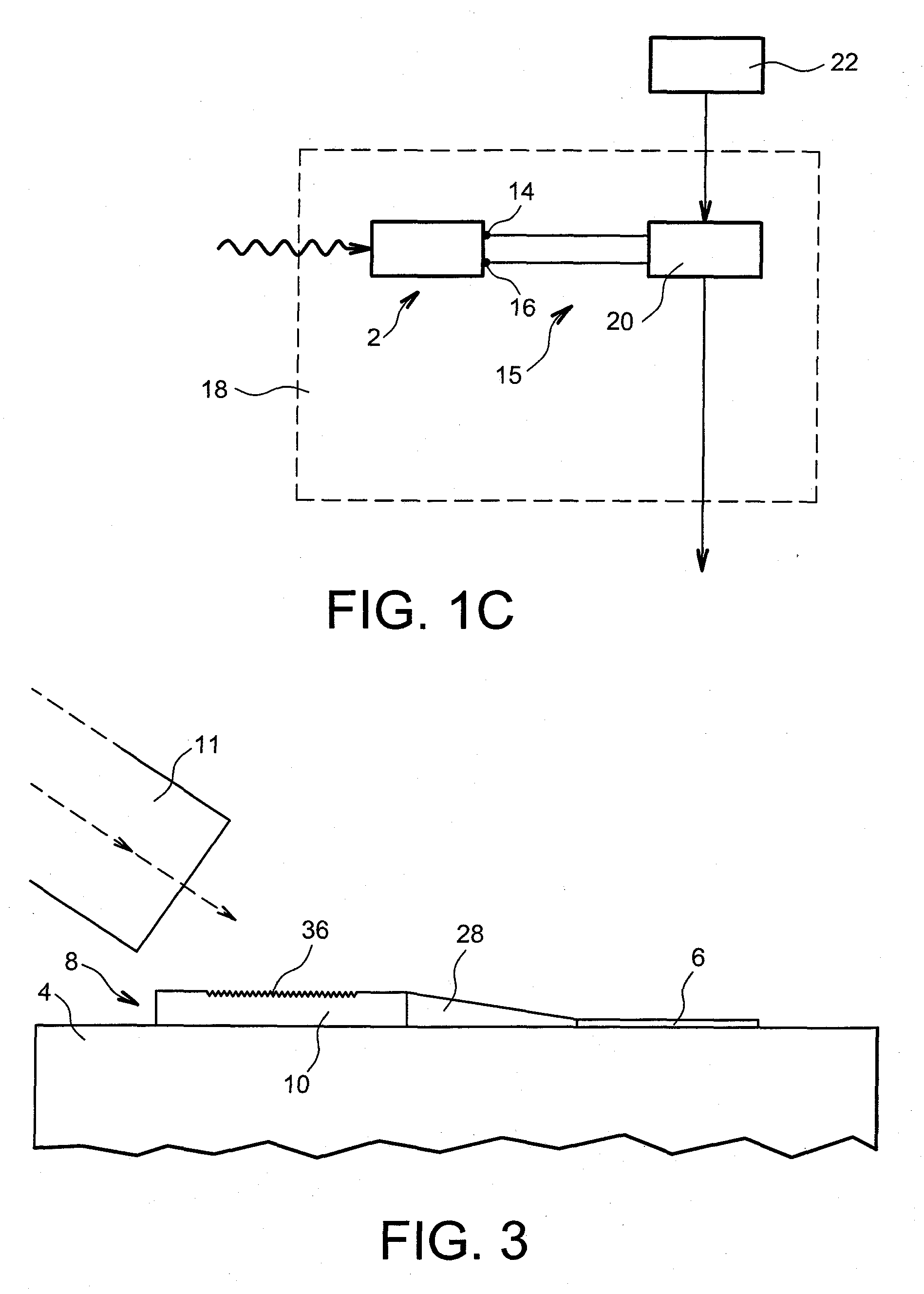
[0078]Various detectors according to the invention as well as the operation of these detectors, are described hereafter, in the case of a focused incident light beam and then of a collimated incident light beam.

[0079]Let us place ourselves first of all within the scope of a focused incident beam, the width of which is typically a few micrometers and which stems from a single-mode optical fiber or from focusing optics such as for example a microscope objective.

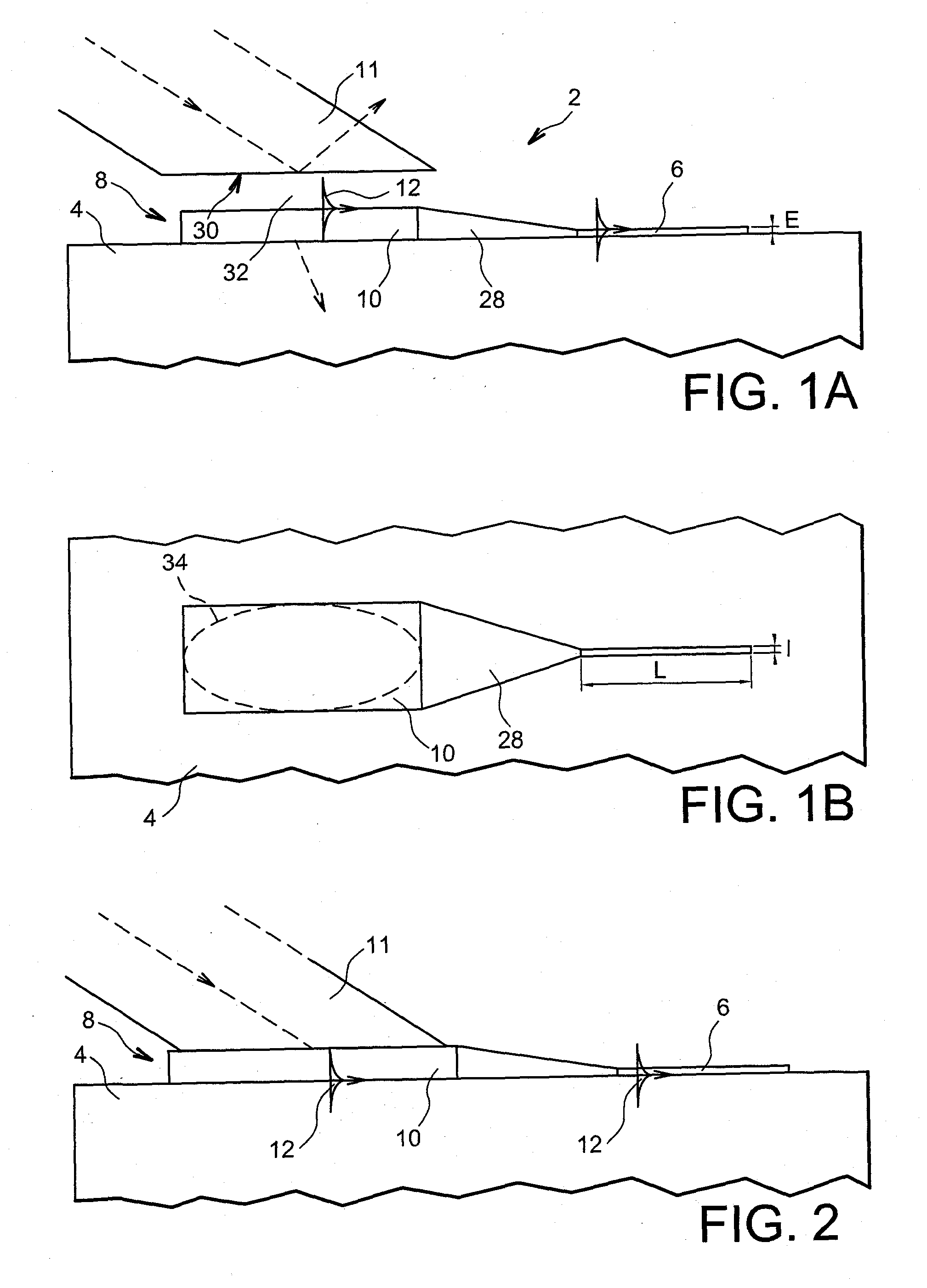
[0080]A first detector example according to the invention is seen in a longitudinal sectional view in FIG. 1A and in a top view in FIG. 1B.

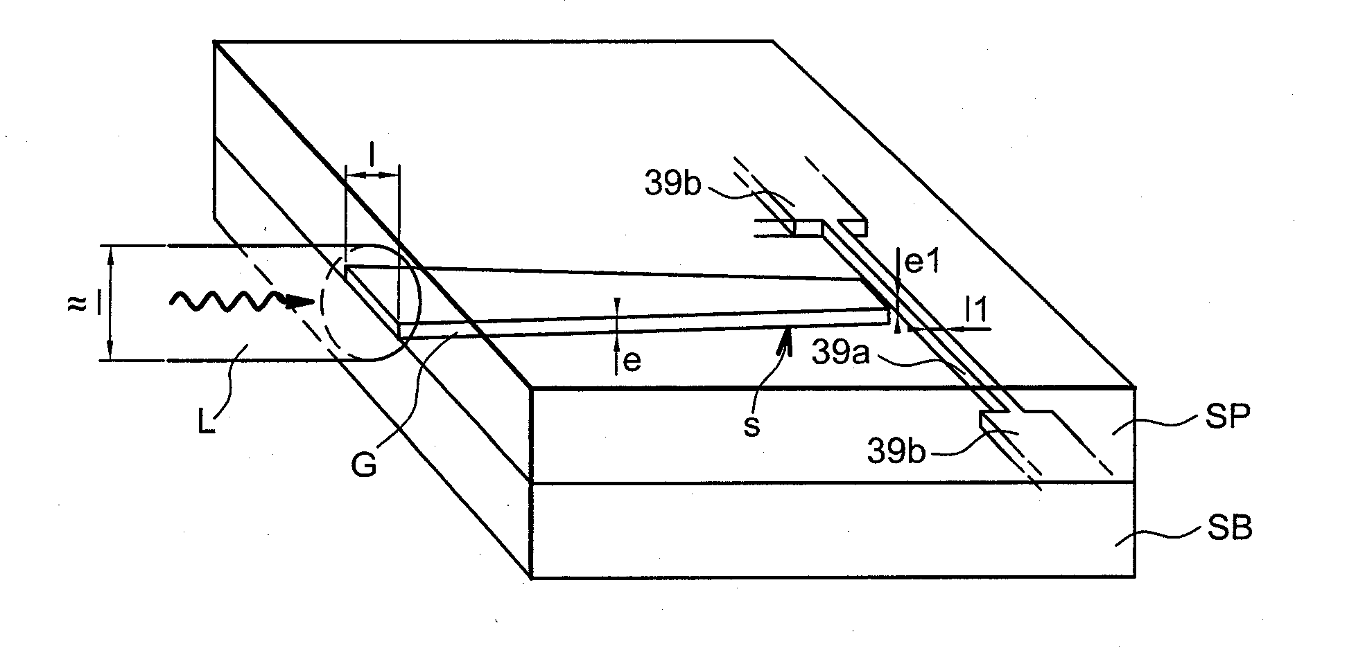
[0081]This detector 2 comprises a dielectric substrate 4 and a bolometric detection component 6 formed on this substrate and made in superconducting material, preferably NbN. This component forms a thin, short and substantially rectilinear strip.

[0082]Typically, the thickness E of this strip is less than 10 nm, its width 1 is less than 1 μm and its length L is less than 100 μm but advantageo...


PUM


Abstract

An ultra-sensitive optical detector with large time resolution, using a surface plasmon. The optical detector is configured to detect at least one photon, and including a dielectric substrate, and on the substrate, at least one bolometric detection component, that generates an electrical signal from the energy of received photon(s). Additionally, at least one coupling component is formed on the substrate, distinct from the detection component and including a metal component, and generates a surface plasmon by interaction with the photon(s) and guiding the plasmon right up to the detection component, which then absorbs the energy of the surface plasmon.

Description

TECHNICAL FIELD[0001]The present invention concerns an ultra-sensitive optical detector with large time resolution, and notably a superconducting single photon detector.[0002]The invention is notably applied to the detection and to the localization of faults in the operation of a semiconducting integrated circuit, by detecting the emission of specific photons by faulty transistors.[0003]It also applies to receiving and routing circuits for very high throughput telecommunications, in particular to those which are intended for telecommunications satellites, because of the very small heat dissipation of the detector, object of the invention.[0004]The invention further applies to detecting the key of the quantum code in a cryptography system.[0005]It also applies to detecting biological or medical objects by tomography as well as to the astronomical observation of remote objects.STATE OF THE PRIOR ART[0006]Emerging techniques such as quantum computation and cryptography, detection of ve...

Claims


Application Information

Patent Timeline
Patent Type & Authority Applications(United States)
IPC IPC(8): G01J1/04
CPCB82Y20/00G01J1/0209G02B2006/12107G02B6/1226G02B6/30G01J1/42
Inventor FREY, LAURENTVILLEGIER, JEAN-CLAUDE
Owner COMMISSARIAT A LENERGIE ATOMIQUE ET AUX ENERGIES ALTERNATIVES
Why Eureka
Try Eureka