Nitride-Based Semiconductor Device and Method for Fabricating the Same

a technology of nitride and semiconductors, applied in semiconductor devices, semiconductor lasers, lasers, etc., can solve the problems of reducing the production yield of devices, difficult to make highly reliable semiconductor lasers, and often scratching of the surface of gan wafers, so as to increase reliability and production yield, reduce the resistance to current flowing across the principal surface of the substra

Inactive Publication Date: 2008-11-06
PANASONIC CORP
View PDF8 Cites 60 Cited by
  • Summary
  • Abstract
  • Description
  • Claims
  • Application Information

AI Technical Summary

Benefits of technology

[0043]According to the present invention, electrical resistance to a current flowing across the principal surface of a substrate can be reduced, t...

Problems solved by technology

If the dislocation density is that high, it is difficult to make highly reliable semiconductor lasers.
Such unevenness on the principal surface of a GaN wafer will pose a big obstacle to a photolithographic process, for example, thus decreasing the production yield of devices.
In that case...

Method used


Image

  • Nitride-Based Semiconductor Device and Method for Fabricating the Same
  • Nitride-Based Semiconductor Device and Method for Fabricating the Same
  • Nitride-Based Semiconductor Device and Method for Fabricating the Same

Examples


embodiment 1

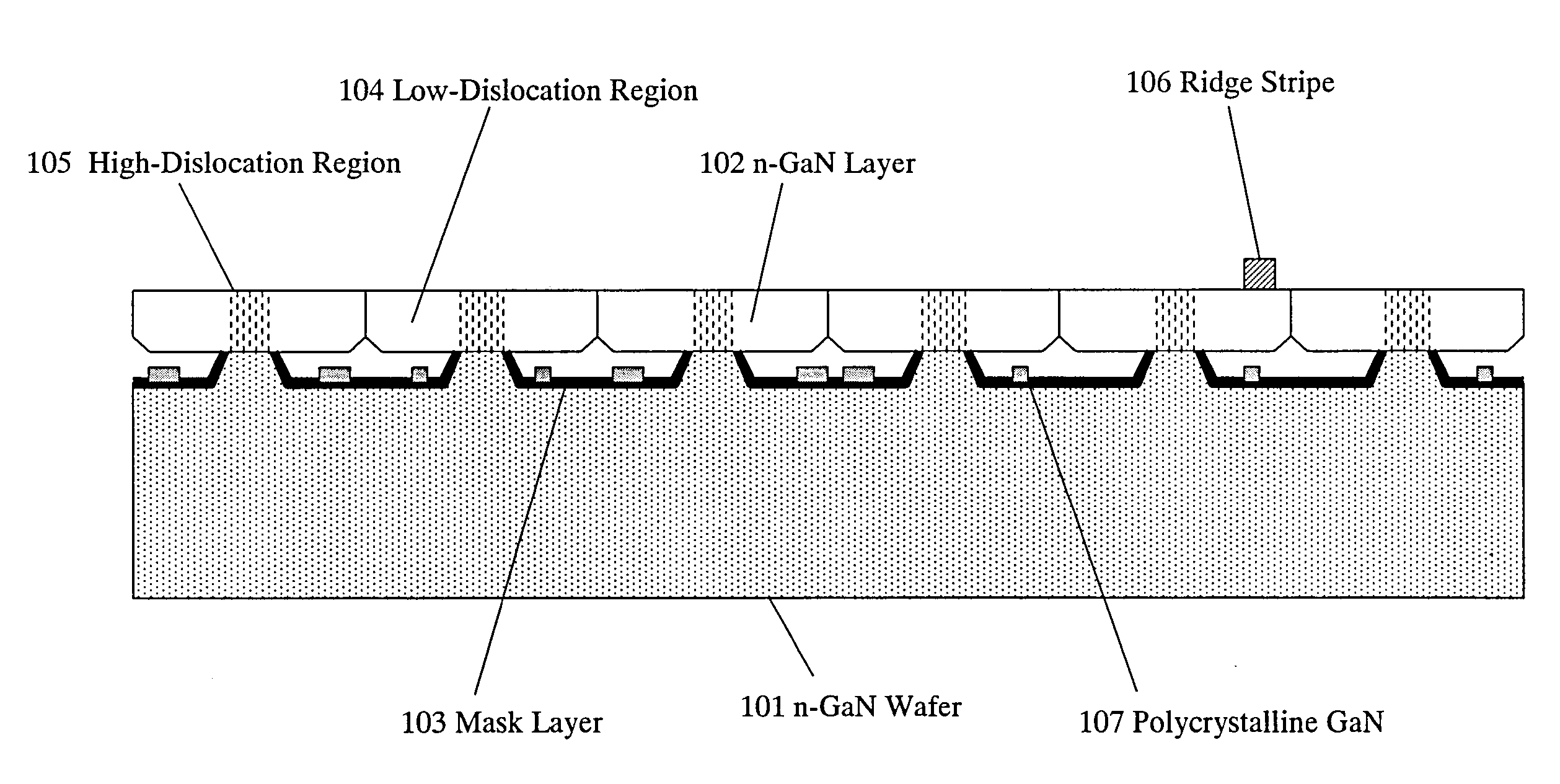
[0099]First, referring to FIG. 1, illustrated schematically is a cross section of a nitride-based semiconductor device according to a first specific preferred embodiment of the present invention.

[0100]The semiconductor device shown in FIG. 1 includes a GaN substrate 101 including multiple striped ridges on the principal surface thereof and an n-GaN layer 102 that has grown on the GaN substrate 101. In an actual semiconductor device, a number of nitride-based semiconductor layers are usually stacked one upon the other on the n-GaN layer 102. However, if the n-GaN layer 102 shown in FIG. 1 is used as a channel layer for transistors, a gate insulating film, an interconnect structure and so on are formed on the n-GaN layer 102.

[0101]The configuration of the GaN substrate 101 will be described in further detail with reference to FIG. 2. Specifically, FIG. 2(a) is a top view illustrating the principal surface of the GaN substrate 101 of a nitride-based semiconductor device and FIG. 2(b) i...

embodiment 2

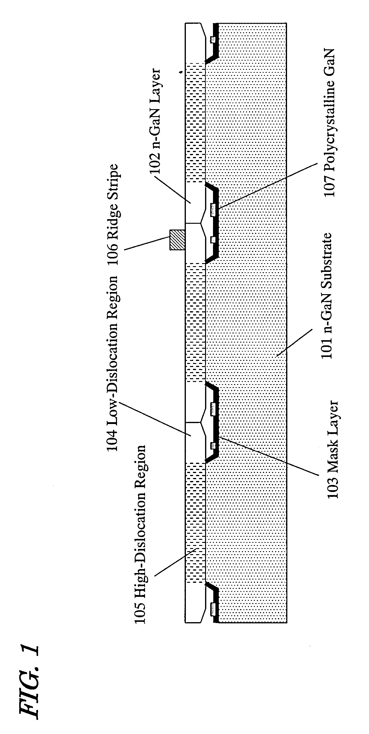
[0131]Hereinafter, a second preferred embodiment of a nitride-based semiconductor device according to the present invention will be described with reference to FIG. 6, which schematically illustrates a cross-sectional structure of a nitride semiconductor laser according to this preferred embodiment.

[0132]The semiconductor laser illustrated in FIG. 6 includes an n-GaN substrate 101 with a striped recess on its principal surface and a semiconductor multilayer structure that has been grown on the GaN substrate 101. The lowermost layer of the semiconductor multilayer structure is an n-GaN layer 102 that has been grown on the n-GaN substrate 101. The n-GaN substrate 101 and the n-GaN layer 102 of this preferred embodiment are made by the same method as the counterparts of the first preferred embodiment described above.

[0133]The semiconductor multilayer structure is formed by stacking an n-AlGaN / GaN superlattice contact layer 201, an n-AlGaN / GaN superlattice cladding layer 202, an n-GaN o...

embodiment 3

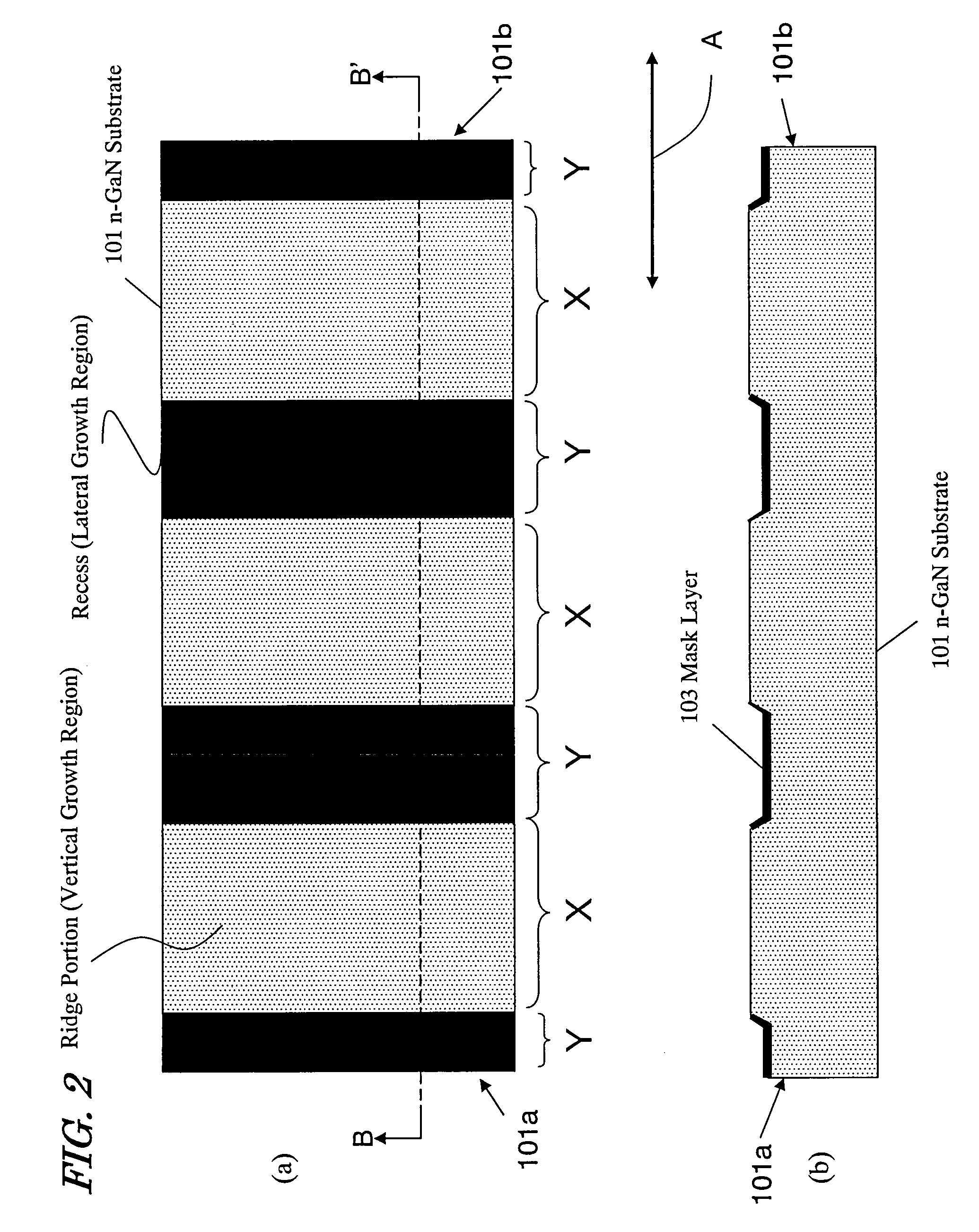
[0141]Hereinafter, a third preferred embodiment of a nitride-based semiconductor device according to the present invention will be described with reference to FIG. 8.

[0142]The arrangement of this preferred embodiment is different from that shown in FIG. 1 in that a GaN layer 801 (with a thickness of 1 μm) is further provided on the surface of the n-GaN substrate 101 according to this preferred embodiment. Specifically, after the GaN layer 801 has been grown on the principal surface of the n-GaN wafer 101, a striped ridge is formed on the principal surface of the wafer by the method that has already been described for the first preferred embodiment.

[0143]In this preferred embodiment, the ridge portion (corresponding to a raised portion of the resist) has a width X of about 20 μm and the recess has a width Y of about 5 μm. The bottom and side surface of the recess are covered with a mask layer 103 of SiO2 that has been deposited by ECR sputtering process or thermal CVD process.

[0144]T...


PUM


Abstract

A nitride-based semiconductor device according to the present invention includes a semiconductor multilayer structure supported on a substrate structure 101 with electrical conductivity. The principal surface of the substrate structure 101 has at least one vertical growth region, which functions as a seed crystal for growing a nitride-based semiconductor vertically, and a plurality of lateral growth regions for allowing the nitride-based semiconductor that has grown on the vertical growth region to grow laterally. The sum ΣX of the respective sizes of the vertical growth regions as measured in the direction pointed by the arrow A and the sum ΣY of the respective sizes of the lateral growth regions as measured in the same direction satisfy the inequality ΣX/ΣY>1.0.

Description

TECHNICAL FIELD[0001]The present invention relates to a nitride-based semiconductor device such as a semiconductor laser that can be used in the fields of optical information processing and displays and also relates to a method for fabricating such a device.BACKGROUND ART[0002]A violet semiconductor laser, made of Group III-V nitride semiconductors (AlxGayIn1-x-yN (where 0≦x≦1 and 0≦y≦1) such as gallium nitride (GaN), is a key device for realizing ultrahigh density recording by optical disk drives, and is about to be actually used in consumer electronics products. The output of a violet semiconductor laser must be increased not just to enable high-speed writing on an optical disk but also to develop new fields of technology including application to laser displays. A conventional violet semiconductor laser is disclosed in Non-Patent Document No. 1, for example.[0003]Recently, a GaN wafer has been regarded as a strong candidate for a wafer for fabricating a nitride-based semiconductor...

Claims


Application Information

Patent Timeline
IPC IPC(8): H01L21/20H01L29/201
CPCH01L21/02389H01L21/0254H01L21/0262H01L21/02639H01L21/0265H01S5/22H01S5/32341H01S2304/12
Inventor SHIMAMOTO, TOSHITAKAKAWAGUCHI, YASUTOSHIHASEGAWA, YOSHIAKIISHIBASHI, AKIHIKOKIDOGUCHI, ISAOYOKOGAWA, TOSHIYA
Owner PANASONIC CORP
Why Eureka
Try Eureka