Data transfer circuit, solid-state imaging device and camera system

Active Publication Date: 2008-11-06
SONY CORP
View PDF9 Cites 12 Cited by
  • Summary
  • Abstract
  • Description
  • Claims
  • Application Information

AI Technical Summary

Benefits of technology

[0029]Accordingly, it is desirable to provide a data transfer circuit, solid-state imaging device and camera system, which can reduce the parasitic capacitance and / or parasitic resistance on a transfer line to a data detecting circuit and can increase the speed of the data transfer to the data detecting circuit.
[0036]According to the embodiments of the invention, the parasitic capacitance and / or parasitic resistance on a transfer line to a data detecting circuit can be reduced.
[0037]Therefore, the speed of the data transfer to the data detecting circuit can be increased.

Problems solved by technology

However, the horizontal transfer line in a solid-state imaging device (CMOS image sensor) as described above is significantly long and may have a length of about 7 mm, and the detection time varies between the sides near and far away from the sense circuit due to the parasitic capacitance and / or resistance.
As a result, it is important to tune the sense circuit to allow the variations, which disadvantageously complicates the circuit design.
There is also a problem of mixing of digital noise from the memory device, which is a digital circuit.

Method used


Image

  • Data transfer circuit, solid-state imaging device and camera system
  • Data transfer circuit, solid-state imaging device and camera system
  • Data transfer circuit, solid-state imaging device and camera system

Examples


Embodiment Construction

[0049]In relation to drawings, embodiments of the invention will be described below.

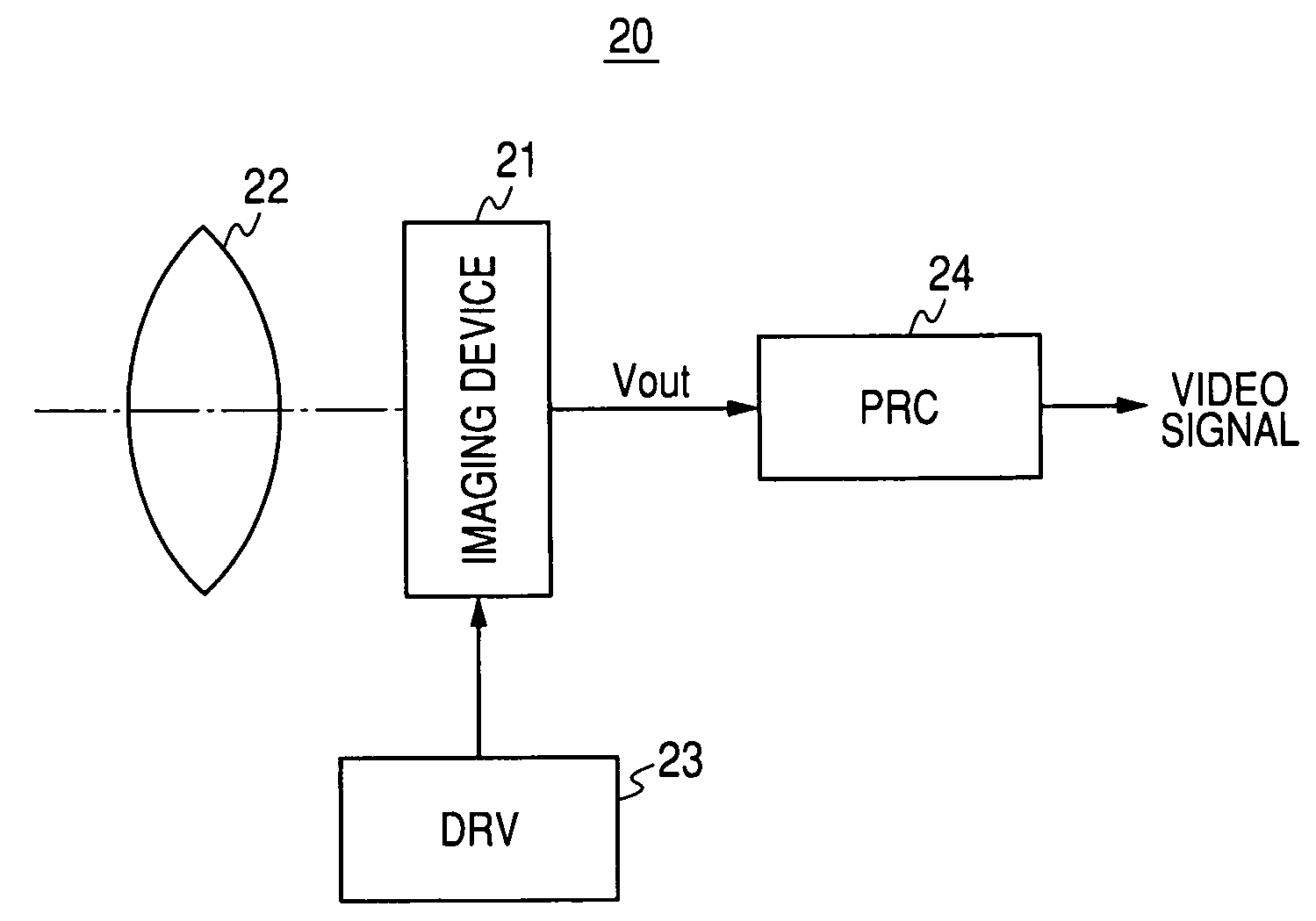
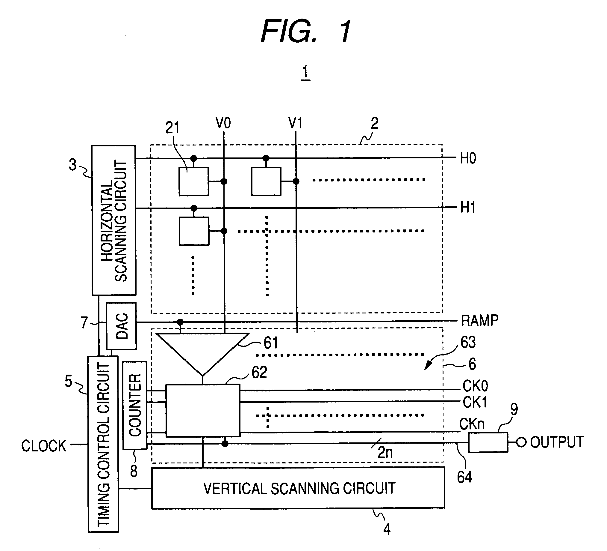
[0050]FIG. 3 is a block diagram showing a configuration example of a solid-state imaging device (CMOS image sensor) having a column parallel ADC, which includes a data transfer circuit according to an embodiment of the invention. FIG. 4 is a diagram showing a more specific configuration example of a data transfer system of the ADC and sold-state imaging device in FIG. 3.

[0051]A solid-state imaging device 10 has a pixel array section 11 functioning as an imaging section, a horizontal scanning circuit 12, a vertical scanning circuit 13 (-0 to -i to -n), a timing control circuit 14, an ADC group 15, a DAC 16 and multiple sense amplifiers (S / A) circuits 17, which function as a data detecting circuit.

[0052]The pixel array section 11 has unit pixels ill each containing a photodiode and an in-pixel amplifier. The unit-pixels 111 are laid out in a matrix form of M rows by N columns.

[0053]The solid-state imag...


PUM


Abstract

A data transfer circuit includes at least one transfer line transferring digital data, at least one data detecting circuit connecting to the transfer line, multiple holding circuits holding a digital value corresponding to the input level and transferring the digital value to the transfer line, and a scanning circuit selecting the multiple holding circuits, wherein the multiple holding circuits are laid out in parallel, and the transfer line is placed in the direction orthogonal to the direction of the parallel layout of the holding circuit and connects to the data detecting circuit placed in the orthogonal direction.

Description

CROSS REFERENCES TO RELATED APPLICATIONS[0001]The present invention contains subject matter related to Japanese Patent Application JP 2007-121408 filed in the Japanese Patent Office on May 2, 2007, the entire contents of which being incorporated herein by reference.BACKGROUND OF THE INVENTION[0002]1. Field of the Invention[0003]The present invention relates to a data transfer circuit, a solid-state imaging device typically such as a CMOS image sensor and a camera system and, in particular, to a solid-state imaging device and camera system that include a column parallel analog-digital converter.[0004]2. Description of the Related Art[0005]A CMOS image sensor having a column parallel analog-digital converter (which will be abbreviated to ADC hereinafter) is proposed in W. Yang et al., “An Integrated 800×600 CMOS Image System,” ISSCC Digest of Technical Papers, pp. 304-305, February 1999 (Non-Patent Document 1).[0006]FIG. 1 is a block diagram showing a configuration example of a solid-...

Claims


Application Information

Patent Timeline
IPC IPC(8): H04N5/335H03K17/62H01L27/146H04N5/341H04N5/357H04N5/369H04N5/374
CPCH03K17/6871H03K17/6872H04N5/3745H04N5/3355H03K17/78H04N25/77H04N25/78H04N25/772
Inventor TAURA, TADAYUKI
Owner SONY CORP
Why Eureka
Try Eureka