Surface treatment method

a surface treatment and surface technology, applied in the direction of grinding machines, edge grinding machines, manufacturing tools, etc., can solve the problems of inability to control the temperature of wafers with good response, minute undulations on the surface of electrostatic chucks, and high power consumption, so as to improve the efficiency of heat transfer

Active Publication Date: 2008-11-13
TOKYO ELECTRON LTD
View PDF7 Cites 19 Cited by
  • Summary
  • Abstract
  • Description
  • Claims
  • Application Information

AI Technical Summary

Benefits of technology

[0012]It is an object of the present invention to provide a surface treatment method that enables a surface of an electrostatic chuck to be smoothed, so as to improve the efficiency of heat transfer between the surface of the electrostatic chuck and a substrate.
[0014]According to the above surface treatment method, the flatness of the substrate mounting surface is improved, and then the surface whose flatness has been improved is smoothed using tape coated with abrasive grains. As a result, an extreme surface layer of the substrate mounting surface can be smoothed. The contact area between a substrate and a surface of an electrostatic chuck that is the substrate mounting surface can thus be increased, and hence the efficiency of heat transfer between the substrate and the surface of the electrostatic chuck can be markedly improved. When controlling a processing temperature of the substrate, there is thus no need to use a high-performance chiller unit, and hence power saving can be achieved for the chiller unit. Moreover, even in the case that an etching process carried out on the substrate is divided into a plurality of steps, the temperature of the substrate can be controlled with good response when changing steps, and hence the requirements of a variety of etching characteristics can be met. Furthermore, because the efficiency of heat transfer between the substrate and the surface of the electrostatic chuck can be markedly improved, even in the case of wishing to reduce the temperature of the substrate, there is no need to excessively increase the pressure of a heat transfer gas, and hence detachment of the substrate from the electrostatic chuck can be prevented.
[0016]According to the above surface treatment method, the substrate mounting surface is flattened using a grindstone, and then the flattened surface is further flattened using a plate coated with abrasive grains. As a result, the flatness of the substrate mounting surface can be further improved. The efficiency of heat transfer between the substrate and the surface of the electrostatic chuck can thus be further improved, and hence power saving can be achieved for the chiller unit, and the requirements of a variety of etching characteristics can be met.
[0018]According to the above surface treatment method, the substrate mounting surface has a sprayed coating film formed thereon. As a result, the flatness of the substrate mounting surface can be improved easily, and the extreme surface layer of the substrate mounting surface can be smoothed easily.
[0020]According to the above surface treatment method, the flatness of the surface of the sprayed coating film is improved, and then the surface whose flatness has been improved is smoothed using tape coated with abrasive grains. As a result, an extreme surface layer of the sprayed coating film can be smoothed. For the member having the sprayed coating film formed thereon, contact heat transfer from the member to an adjacent member can thus be increased, and hence, for example, the adjacent member can be made to be at the same temperature as the member, or the temperature of a member not provided with a coolant chamber through which a coolant is directly passed can be controlled. In this case, if at least one of the mutually adjacent members is processed using the surface treatment method, then effects as for the surface treatment method in the first aspect of the present invention can be obtained for both of the mutually adjacent members.
[0022]According to the above surface treatment method, the surface of the sprayed coating film is flattened using a grindstone, and then the flattened surface is further flattened using a plate coated with abrasive grains. As a result, the flatness of the sprayed coating film can be further improved. The contact heat transfer between the mutually contacting members can thus be further increased.

Problems solved by technology

However, as shown in FIG. 4D, an electrostatic chuck processed using the conventional method has a rough surface when viewed microscopically, and furthermore there are minute undulations on the surface of the electrostatic chuck.
To achieve both high-density, high-ion energy plasma and a low wafer temperature, it is thus necessary to use a chiller unit that can produce an extremely low temperature and hence has a high power consumption.
Moreover, in recent years, due to etched shapes becoming finer and more complex, etching processes have come to be divided into a plurality of steps, it being required to control the wafer temperature with good response when changing steps.
However, in the case of a conventional electrostatic chuck, because the thermal contact resistance between the wafer and the surface of the electrostatic chuck is high, the wafer temperature cannot be controlled with good response by controlling the temperature of the coolant from the chiller unit.
Moreover, even in the case of using, for example, a heater or a Peltier element as a temperature control device for the wafer in the electrostatic chuck, the wafer temperature still cannot be controlled with good response.
However, with this method, to satisfy the above requirements on the etching characteristics, the pressure of the heat transfer gas must be greatly increased, so that in some cases the wafer may become detached from the electrostatic chuck.
However, in this case, the voltage resistance of the insulating member of the electrostatic chuck must be increased, and setting the thickness of the insulating member which is a layer above the electrode plate in the electrostatic chuck so as to achieve both a good wafer attracting force and a good insulating member voltage resistance is difficult from a design perspective.
The insulating member generally has a worse heat transfer coefficient than a metal, and hence if the insulating member is made thicker so as to increase the voltage resistance, then there is a problem that the efficiency of heat transfer becomes poor in this region.

Method used


Image

  • Surface treatment method
  • Surface treatment method
  • Surface treatment method

Examples


first embodiment

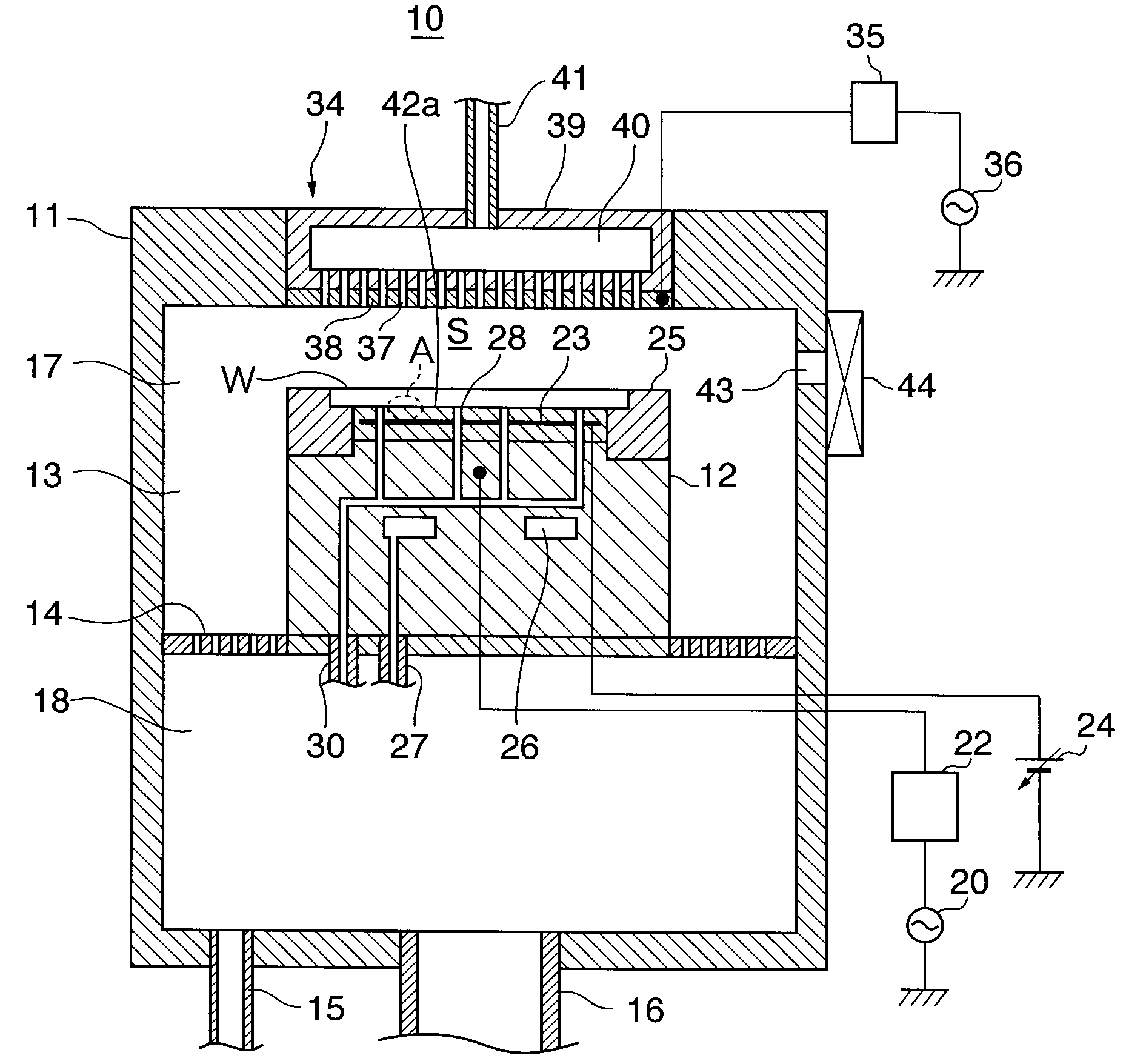
[0040]First, a substrate processing apparatus having therein an electrostatic chuck processed using a surface treatment method according to the present invention will be described.

[0041]FIG. 1 is a sectional view schematically showing the construction of the substrate processing apparatus having therein the electrostatic chuck processed using the surface treatment method according to the first embodiment of the present invention. The substrate processing apparatus is constructed such as to carry out etching processing on a semiconductor wafer as a substrate.

[0042]As shown in FIG. 1, the substrate processing apparatus 10 has a chamber 11 in which is housed a semiconductor wafer (hereinafter referred to merely as a “wafer”) W having a diameter of, for example, 300 mm. A cylindrical susceptor 12 is disposed in the chamber 11 as a stage on which the wafer W is mounted. In the substrate processing apparatus 10, a side exhaust path 13 that acts as a flow path through which gas above the s...

second embodiment

[0068]Next, a surface treatment method according to the present invention will be described.

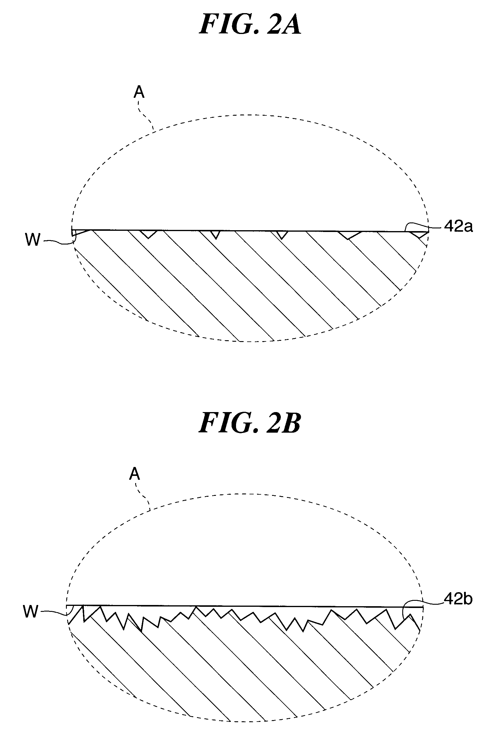
[0069]For the present embodiment, the construction and operation are basically the same as for the first embodiment described above, the only difference to the first embodiment being that the plate lapping step is omitted. Features of the construction and operation that are the same as in the first embodiment will thus not be described, only features of the construction and operation that are different to in the first embodiment being described below with reference to FIGS. 3.

[0070]In the surface treatment method according to the present embodiment, the electrostatic chuck is subjected to the thermal spraying step shown in FIG. 3A, then to the grinding step shown in FIG. 3C, and then to the tape lapping step shown in FIG. 3G.

[0071]In the present embodiment, after the tape lapping step, there are minute undulations on the surface of the electrostatic chuck, but regardless of the state of the u...

third embodiment

[0073]Next, a surface treatment method according to the present invention will be described.

[0074]For the present embodiment, the construction and operation are basically the same as for the first embodiment described above, the only difference to the first embodiment being that the grinding step is omitted. Features of the construction and operation that are the same as in the first embodiment will thus not be described, only features of the construction and operation that are different to those in the first embodiment being described below with reference to FIGS. 3.

[0075]In the surface treatment method according to the present embodiment, the electrostatic chuck is subjected to the thermal spraying step shown in FIG. 3A, then to the plate lapping step shown in FIG. 3E, and then to the tape lapping step shown in FIG. 3G.

[0076]In the present embodiment, after the tape lapping step, the surface of the electrostatic chuck has been flattened, and furthermore the extreme surface layer o...


PUM

PropertyMeasurementUnit
diameteraaaaaaaaaa
pressureaaaaaaaaaa
flatnessaaaaaaaaaa

Abstract

A surface treatment method that enables a surface of an electrostatic chuck to be smoothed, so as to improve the efficiency of heat transfer between the surface of the electrostatic chuck and a substrate. The electrostatic chuck is provided in an upper portion of a susceptor provided in a chamber of a substrate processing apparatus. In the surface treatment of the electrostatic chuck, a sprayed coating film is formed on the surface of the electrostatic chuck, next the surface of the electrostatic chuck is ground by bringing into contact therewith a grindstone, then the surface of the electrostatic chuck is ground flat by bringing into contact therewith a lapping plate onto a surface of which is sprayed a suspension, and then the surface of the electrostatic chuck is ground smooth by bringing into contact therewith a tape of a tape lapping apparatus.

Description

BACKGROUND OF THE INVENTION[0001]1. Field of the Invention[0002]The present invention relates to a surface treatment method, and in particular relates to a surface treatment method for a sprayed coating film formed on a surface of an electrostatic chuck.[0003]2. Description of the Related Art[0004]Substrate processing apparatuses are known that carry out plasma processing such as etching processing on wafers as substrates. Such an apparatus has a housing chamber in which a wafer is housed, and a stage that is disposed in the housing chamber and on which the wafer is mounted. In the substrate processing apparatus, plasma is produced in the housing chamber, and the wafer is subjected to the etching processing by the plasma.[0005]The stage has in an upper portion thereof an electrostatic chuck comprised of an insulating member having an electrode plate therein, the wafer being mounted on the electrostatic chuck. While the wafer is being subjected to the etching processing, a DC voltage...

Claims


Application Information

Patent Timeline
Patent Type & Authority Applications(United States)
IPC IPC(8): B24B1/00
CPCB24B1/00B24B21/04
Inventor SASAKI, YASUHARUHIGUMA, MASAKAZUAOTO, TADASHIKIKUCHI, EIICHIRO
Owner TOKYO ELECTRON LTD
Why Eureka
Try Eureka