Method for growing semiconductor layer, method for producing semiconductor light-emitting element, semiconductor light-emitting element, and electronic device

a technology of light-emitting elements and semiconductors, which is applied in the direction of polycrystalline material growth, crystal growth process, chemically reactive gas, etc., can solve the problems of reducing the probability of electron-hole recombination, reducing the internal quantum efficiency of a light-emitting diode, and reducing the external quantum efficiency. , to achieve the effect of improving crystal quality, reducing piezoelectric field, and improving crystal quality

Inactive Publication Date: 2008-11-20
SONY CORP
View PDF10 Cites 30 Cited by
  • Summary
  • Abstract
  • Description
  • Claims
  • Application Information

AI Technical Summary

Benefits of technology

[0050]According to the present embodiment, the semiconductor layer can be grown on a substrate in a desired plane direction with a desired growth plane facet, and the resulting semiconductor layer has a suppressed piezoelectric field and an improved crystal quality. The method for growing the semiconductor layer can be applied to the growth of the semiconductor layers as the constituents of the light-emitting element, and the resulting semiconductor layer has an improved crystal quality and a suppressed quantum confined Stark effect in the active layer. The semiconductor light-emitting element can be produced more easily than that disclosed in Patent Document 1. The high-performance semiconductor element can be used to realize a variety of electronic equipment such as high-performance backlight, illuminator, and display.

Problems solved by technology

Unfortunately, when grown on the (0001) plane (or C-plane) of a sapphire substrate, the pseudomorphic quantum well layer of InGaN oriented in the C axis suffers the disadvantage that a large piezoelectric field occurs in the direction perpendicular to the well plane (or the C axis direction), thereby spatially separating electrons and holes from each other and reducing the probability of electron-hole recombination (which is known as the quantum confined Stark effect).
The result is a decrease in internal quantum efficiency in a light-emitting diode based on InGaN / GaN, which in turn leads to a decrease in external quantum efficiency.
This is one cause to impede improvement in the light-emitting output.
Unfortunately, the GaN semiconductor layer with the (11-20) plane has many threading dislocations which deteriorate its crystal quality.
The existing semiconductor light-emitting element as shown in FIG. 39 permits the multiple quantum well layer 104 as an active layer to decrease in piezoelectric field; however, it suffers the disadvantage that it is not typically easy in practice to grow under good control the multiple quantum well layer 104 with the oblique facet of the {2-1-14} plane or {01-12} plane.
Therefore, it presents difficulties in its efficient production.

Method used


Image

  • Method for growing semiconductor layer, method for producing semiconductor light-emitting element, semiconductor light-emitting element, and electronic device
  • Method for growing semiconductor layer, method for producing semiconductor light-emitting element, semiconductor light-emitting element, and electronic device
  • Method for growing semiconductor layer, method for producing semiconductor light-emitting element, semiconductor light-emitting element, and electronic device

Examples


first embodiment

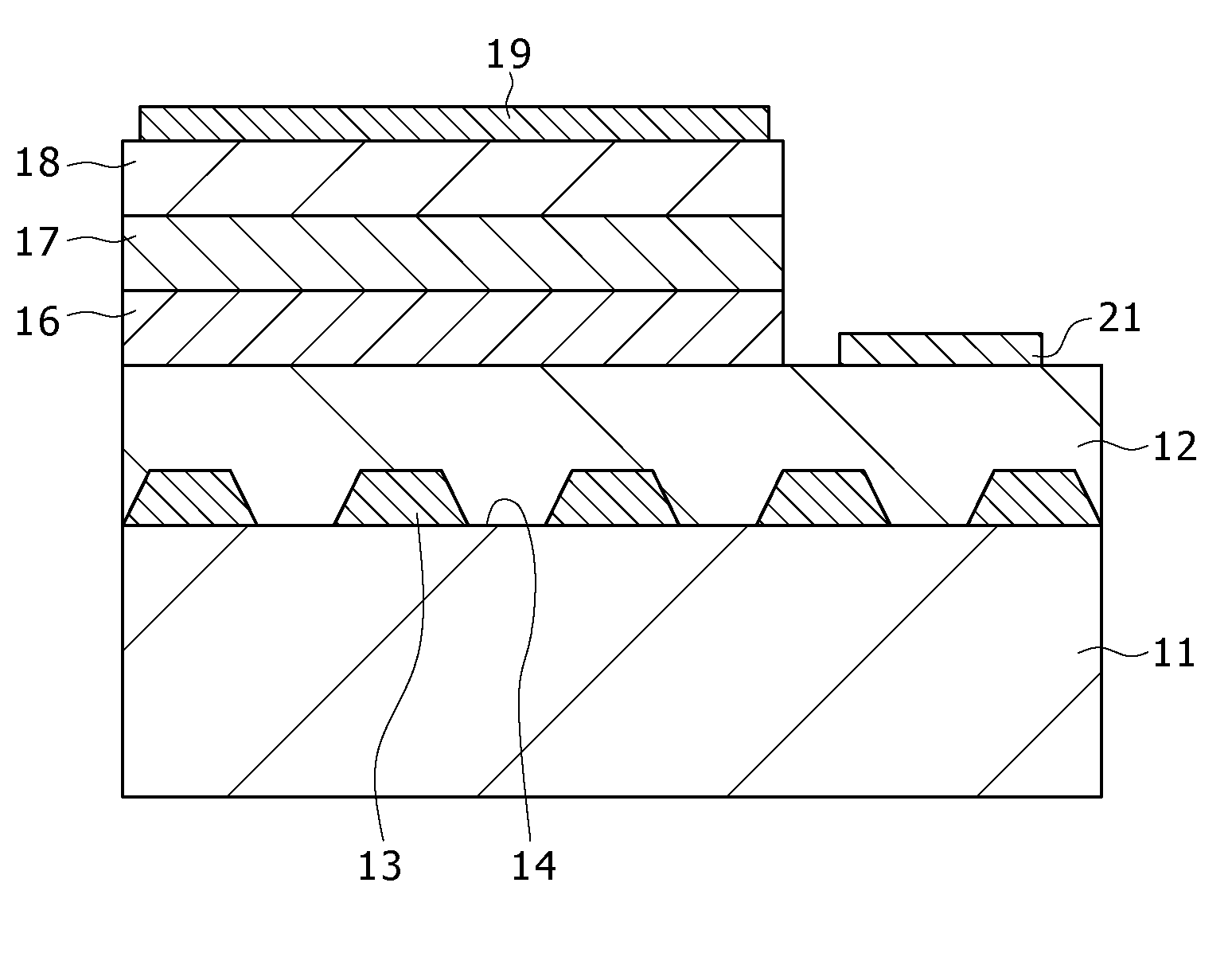
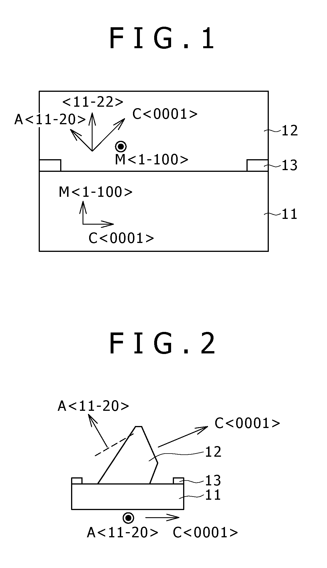
[0091]the present invention, which is illustrated in FIG. 1, is concerned with a basic method for growing a III-V nitride compound semiconductor layer.

[0092]According to the first embodiment, the sapphire substrate 11, whose principal plane is the (1-100) plane (or M-plane), permits the growth thereon of the III-V nitride compound semiconductor layer 12 having the (11-22) plane direction. The sapphire substrate 11 has the raised parts 13 extending straight in one direction, which have been previously formed thereon from SiO2 or SiN. The sapphire substrate 11 and the III-V nitride compound semiconductor layer 12 have the crystal orientation indicated in FIG. 1. The III-V nitride compound semiconductor layer 12 may be grown by the MOCVD process, for example.

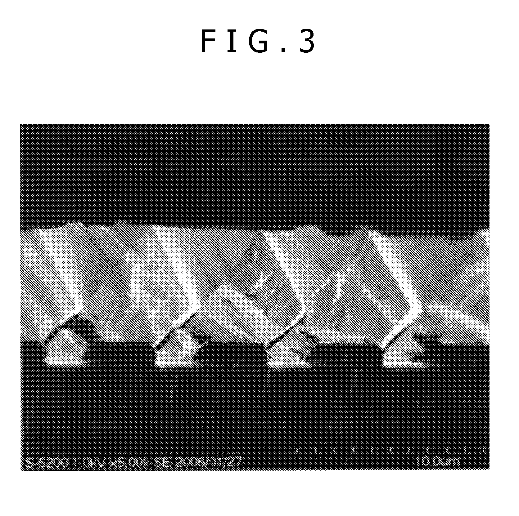
[0093]The III-V nitride compound semiconductor layer 12 in its initial stage of growth is shown in FIG. 2. It grows with its facets orienting in the (11-20) plane (or A-plane), the (0001) plane (or C-plane), and the (11-22) plane. ...

second embodiment

[0103]the present invention, which is illustrated in FIG. 5, is concerned with a basic method for growing a III-V nitride compound semiconductor layer.

[0104]According to the second embodiment, the sapphire substrate 11, whose principal plane is the (1-100) plane (or M-plane), permits the growth thereon of the III-V nitride compound semiconductor layer 12 having the (10-13) plane direction. The sapphire substrate 11 has the raised parts 13 in the same way as in the first embodiment. The sapphire substrate 11 and the III-V nitride compound semiconductor layer 12 have the crystal orientation indicated in FIG. 5. The III-V nitride compound semiconductor layer 12 may be grown by the MOCVD process, for example.

[0105]The III-V nitride compound semiconductor layer 12 in its initial stage of growth is shown in FIG. 6. It grows with its facets facing outward from the (1-100) plane (or M-plane), the (0001) plane (or C-plane), and the (10-13) plane. In this case, its growth in the direction of ...

third embodiment

[0114]the present invention, which is illustrated in FIG. 9, is concerned with a basic method for growing a III-V nitride compound semiconductor layer.

[0115]According to the third embodiment, the sapphire substrate 11, whose principal plane is the (1-102) plane (or R-plane), permits the growth thereon of the III-V nitride compound semiconductor layer 12 having the (11-20) plane direction. The sapphire substrate 11 has the raised parts 13 in the same way as in the first embodiment. The sapphire substrate 11 and the III-V nitride compound semiconductor layer 12 have the crystal orientation indicated in FIG. 9. The III-V nitride compound semiconductor layer 12 may be grown by the MOCVD process, for example.

[0116]The III-V nitride compound semiconductor layer 12 in its initial stage of growth is shown in FIG. 10. In the first example, it grows with its facets facing outward from the (0001) plane (or C-plane) and the (000-1) plane. In the second example, it grows with its facets facing o...


PUM


Abstract

Disclosed herein is a method for growing a semiconductor layer which includes the step of growing a semiconductor layer of hexagonal crystal structure having the (11-22) or (10-13) plane direction on the (1-100) plane of a substrate of hexagonal crystal structure.

Description

CROSS REFERENCES TO RELATED APPLICATIONS[0001]The present invention contains subject matter related to Japanese Patent Application JP 2007-133340 filed in the Japan Patent Office on May 18, 2007, the entire contents of which being incorporated herein by reference.BACKGROUND OF THE INVENTION[0002]1. Field of the Invention[0003]The present invention relates to a method for growing semiconductor layers, a method for producing a semiconductor light-emitting element, a semiconductor light-emitting element, and an electronic device. More particularly, the present invention relates to a III-V nitride compound semiconductor light-emitting diode and a variety of apparatus and equipment provided with the light-emitting diode.[0004]2. Description of the Related Art[0005]The existing method for producing a light-emitting diode based on a GaN semiconductor is mostly by growing an n-type layer, an active layer, and a GaN semiconductor layer including a layer on the (0001) plane (or C-plane) of a ...

Claims


Application Information

Patent Timeline
IPC IPC(8): H01L33/00C30B25/18H01L33/32
CPCC30B25/02C30B25/18H01L21/0242H01L21/02433H01L21/02458H01L33/16H01L21/02609H01L21/0262H01L21/02639H01L21/02647H01L33/007H01L21/0254H01L2224/48465
Inventor OHMAE, AKIRAARIMOCHI, MASAYUKIMITOMO, JUGOFUTAGAWA, NORIYUKIHINO, TOMONORI
Owner SONY CORP
Why Eureka
Try Eureka