Method and apparatus for wafer edge cleaning

a technology of edge cleaning and wafers, applied in the direction of cleaning process and apparatus, chemistry apparatus and processes, cleaning using liquids, etc., can solve the problems of severe defects, yield loss, and inevitably generated defects, so as to reduce the impact of formation, reduce the effect of aging, and be easy to remov

Inactive Publication Date: 2008-11-27
GLOBALFOUNDRIES INC
View PDF17 Cites 25 Cited by
  • Summary
  • Abstract
  • Description
  • Claims
  • Application Information

AI Technical Summary

Benefits of technology

[0010]It is another object of the invention to remove black silicon on a semiconductor wafer while minimally impacting the formation of other severe defects leading to yield loss.
[0011]To achieve these and other objects, aspects and advantages of the invention, the wafer edge is exposed to an irradiation beam, such as a laser beam, after forming deep trenches. The irradiation energy is absorbed by the defects which are heated to a temperature such that the defects melt and are subsequently easily removed. The property that black silicon is an effective absorber of visible and near visible light is used advantageously to produce selective heating and melting. By contrast, a large fraction of the laser energy is reflected from the wafer surface adjacent to black silicon regions. Thus, selective heating, melting and removal of the black silicon without the need for masking is achieved.

Problems solved by technology

In the process of fabricating semiconductor devices, defects are inevitably generated.
These unwanted needle type structures form because dielectrics are left on the surface of the wafer, typically after etching.
During subsequent processing the surface of the wafer is contaminated by the small particles freed from the black silicon, resulting in severe defects and yield loss.
It is known that the edges of the wafer cannot be controllably and uniformly coated with photo-resist, resulting in regions at the edge of the wafer wherein the pad and the hard mask are eroded away during reactive ion etching.
During trench etching, the mask material from adjacent areas is sputtered and deposited on the edge of the wafer which forms a “micro-mask”, that results in the formation of very dense silicon spikes.
The black silicon spikes are formed at the peripheral area of the wafer, and if not removed immediately, could cause wafer contamination and jeopardize yield.
The methods advanced require additional process steps such as film deposition and patterning, which add to the complexity and cost, and further, they are the cause for other defects.
These methods require additional process steps such as deposition, patterning, and removal of the sacrificial material, all of which add to the process complexity and cost, and are the cause of other defect issues.
Although this method may reduce the chance of black silicon formation, it does not completely prevent it.
In addition, the non-standard process to prevent trench patterning at wafer edge may also lead to other process control issues.

Method used


Image

  • Method and apparatus for wafer edge cleaning
  • Method and apparatus for wafer edge cleaning
  • Method and apparatus for wafer edge cleaning

Examples


Embodiment Construction

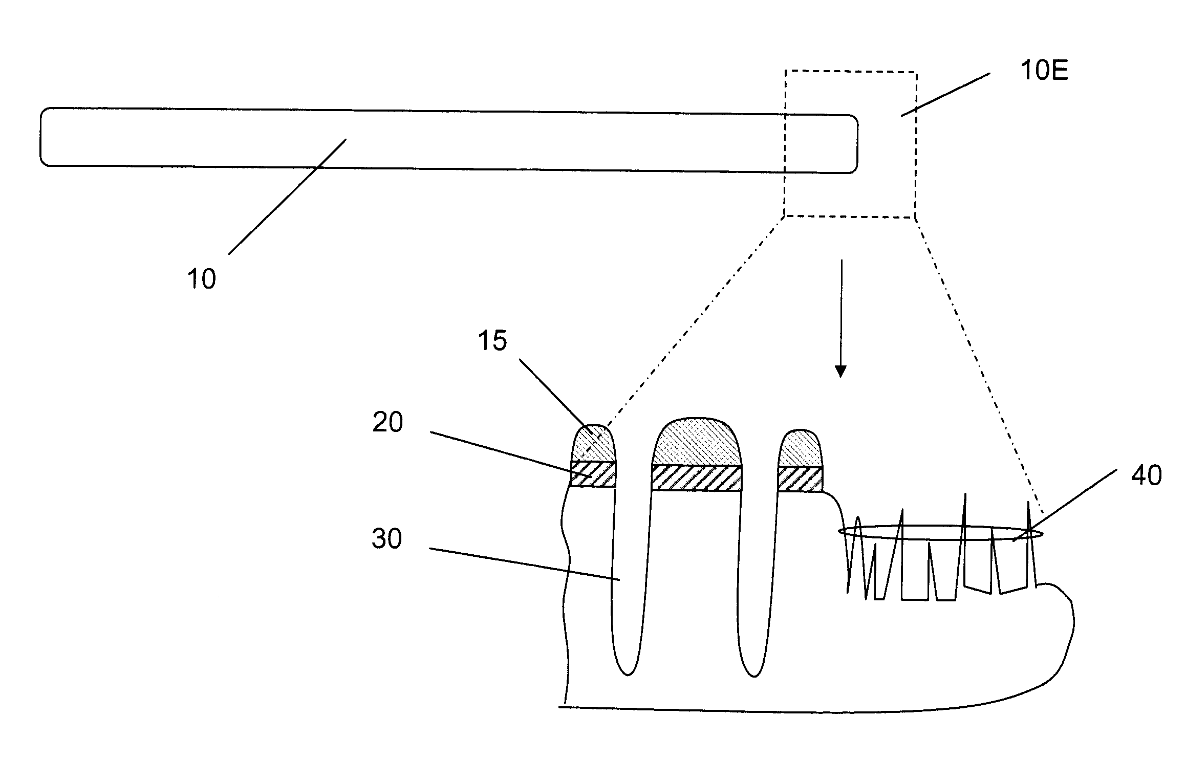
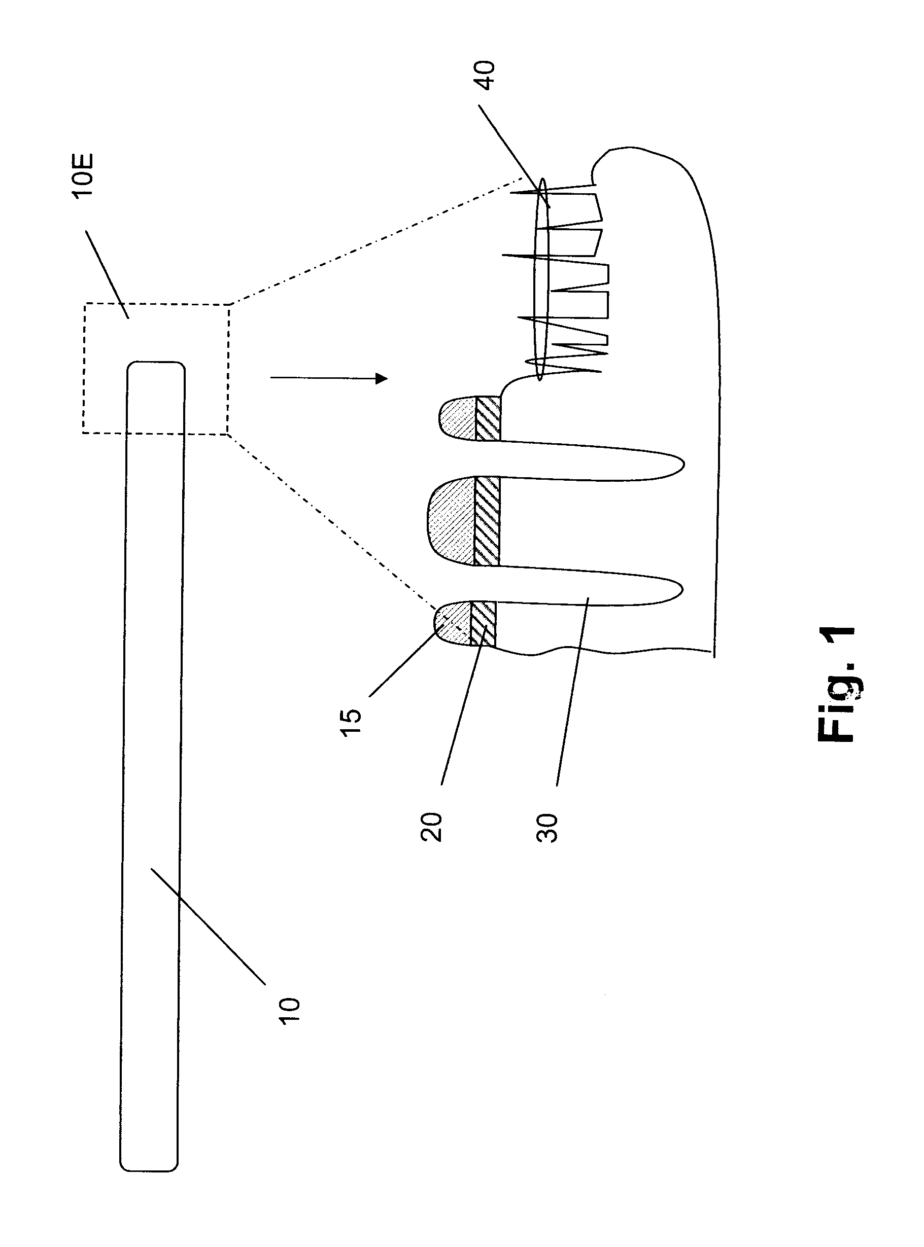
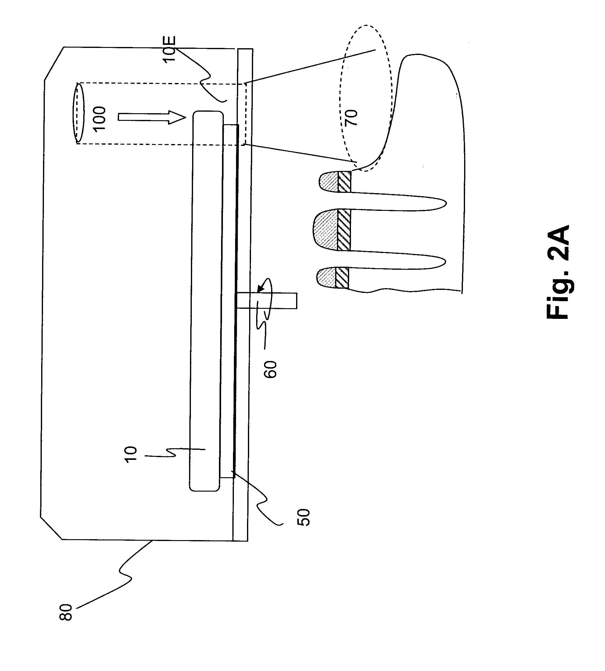
[0021]Referring to FIG. 2, a post-etch wafer 10 is positioned on wafer holder 50 having a spinning post 60. The wafer edge 10E is exposed to a laser beam 100. The wafer is spun at a predetermined rate. The rate of rotation of the wafer may range from about 1 to about 3600 rpm, with 10 to 10 rpm preferred.. Black silicon, which typically becomes amorphous due to ion bombardment during the RIE process, has a lower melting point than single-crystal silicon. It absorbs the light energy and melts, resulting in a smooth profile at the wafer edge. The rough surface which is filled with high-density of spiking structures enhances the light absorption, and results in a rapid meltdown of the back-silicon.

[0022]The preferred source of irradiation is a laser beam. The laser beam can advantageously operate in a continuous wave (CW) or pulsed mode. The wavelength of the laser preferably ranges from 0.1 μm to 20 μm. A XeCl excimer laser having a wavelength of 308 nm is preferably used to melt the ...


PUM

PropertyMeasurementUnit
wavelength rangingaaaaaaaaaa
wavelengthaaaaaaaaaa

Abstract

A wafer edge cleaning system that includes a wafer dry etching chamber and one or more irradiation sources preferably positioned inside the wafer dry etching chamber. The irradiation source such as laser generates a beam aimed at the periphery of the wafer to melt any defects, in particular, black silicon at the edge of the wafer. Preferably, the wafer is mounted on a rotating platform. The invention further provides a method for removing black silicon at the edge of a semiconductor wafer that includes the steps of: patterning the wafer with a trench mask layer; etching the wafer to form a trench thereon; exposing the edge of the wafer to a laser beam to melt the black silicon thereon; stripping the mask and cleaning the wafer.

Description

BACKGROUND OF THE INVENTION[0001]1. Field of the Invention[0002]The present invention relates generally to the field of semiconductor wafer fabrication, and more particularly to a method and a system for removing defects at the edges of a wafer without the need for sacrificial materials and / or patterning.[0003]2. Description of the Prior Art[0004]In the process of fabricating semiconductor devices, defects are inevitably generated. For example, in the process of etching deep trenches in a silicon wafer, a set of silicon spikes 40, referred to as “black silicon”, are formed at the wafer edge as shown in FIG. 1. The name “black silicon” comes from the property that visible light is absorbed by regions containing a high density set of spikes. Black silicon refers to spikes usually about 4 to 8 micrometers in height. These unwanted needle type structures form because dielectrics are left on the surface of the wafer, typically after etching. While some of the dielectric protects the unde...

Claims


Application Information

Patent Timeline
Patent Type & Authority Applications(United States)
IPC IPC(8): B08B6/00
CPCB08B7/0042H01L21/02087H01L21/67069H01L21/67086
Inventor CHENG, KANGGUOHSU, LOUIS C.MANDELMAN, JACK A.
Owner GLOBALFOUNDRIES INC
Why Eureka
Try Eureka