Dynamic random access memory and manufacturing method thereof

a random access and memory technology, applied in the direction of semiconductor devices, electrical devices, transistors, etc., can solve the problems of increasing leakage, reducing the on current of transistors, and affecting the performance of components, so as to improve the effect of components

Active Publication Date: 2008-11-27
NAN YA TECH
View PDF7 Cites 2 Cited by
  • Summary
  • Abstract
  • Description
  • Claims
  • Application Information

AI Technical Summary

Benefits of technology

[0008]Accordingly, the present invention is directed to a dynamic random access memory (DRAM) and a manufacturing method thereof for solving the short channel effect and the floating body effect, so as to enhance the effectiveness of components.
[0015]The channel region of the vertical transistor of the DRAM is disposed in the substrate on sidewalls of the trench between the first doped region and the second doped region. Therefore, the gate width of the vertical transistor on the substrate can be reduced to improve the integration of the component. Moreover, the length of the channel region of the vertical transistor can be accurately controlled by adjusting the depth of the trench, such that the short channel effect and other problems due to miniaturization of the components can be avoided. In addition, since the first doped region of the vertical transistor is adjoined to the upper electrode of the trench capacitor, the doping concentration of the buried strap can be designed according to the processing criteria, such that the floating body effect caused by abnormal contact between the buried doped region and the adjacent deep trench due to excessive doping concentration of the buried strap can be avoided.
[0023]According to an embodiment of the present invention, the second trench may be formed by the following process. First, a patterned second mask layer is formed using the deep trench as an alignment reference object. Then, the second trench is formed using the patterned second mask layer as an etching mask. Therefore, the misalignment usually occurring due to an overlay error between the deep trench and the gate can be avoided, and the process windows may be increased. Moreover, since the length of the channel region of the vertical transistor is determined by the depth of the trench, the length of the channel region of the vertical transistor will not be limited to the photolithographic etching process, therefore the integration of components can be improved. Meanwhile, during the formation of the buried strap, the doping concentration of the buried strap can be designed only according to the processing criteria, and improvement of the doping concentration is unnecessary, such that the floating body effect due to excessive doping concentration of the buried strap can be avoided.

Problems solved by technology

However, this will cause a serious short channel effect and a reduction of the on current of the transistor.
However, this method may also increase the leakage, and therefore reduce the reliability of components.
Moreover, a conventional DRAM has a narrow process window, misalignment usually occurs due to an overlay error between the deep trench and the gate.
However, the doping concentration of the buried strap is generally increased to ensure the buried strap electrically connecting the vertical transistor, and this will cause a floating body effect due to abnormal contact between the buried strap and the adjacent deep trench.
This problem may reduce the reliability and stability of the components.

Method used


Image

  • Dynamic random access memory and manufacturing method thereof
  • Dynamic random access memory and manufacturing method thereof
  • Dynamic random access memory and manufacturing method thereof

Examples


Embodiment Construction

[0028]Reference will now be made in detail to the present preferred embodiments of the invention, examples of which are illustrated in the accompanying drawings. Wherever possible, the same reference numbers are used in the drawings and the description to refer to the same or like parts.

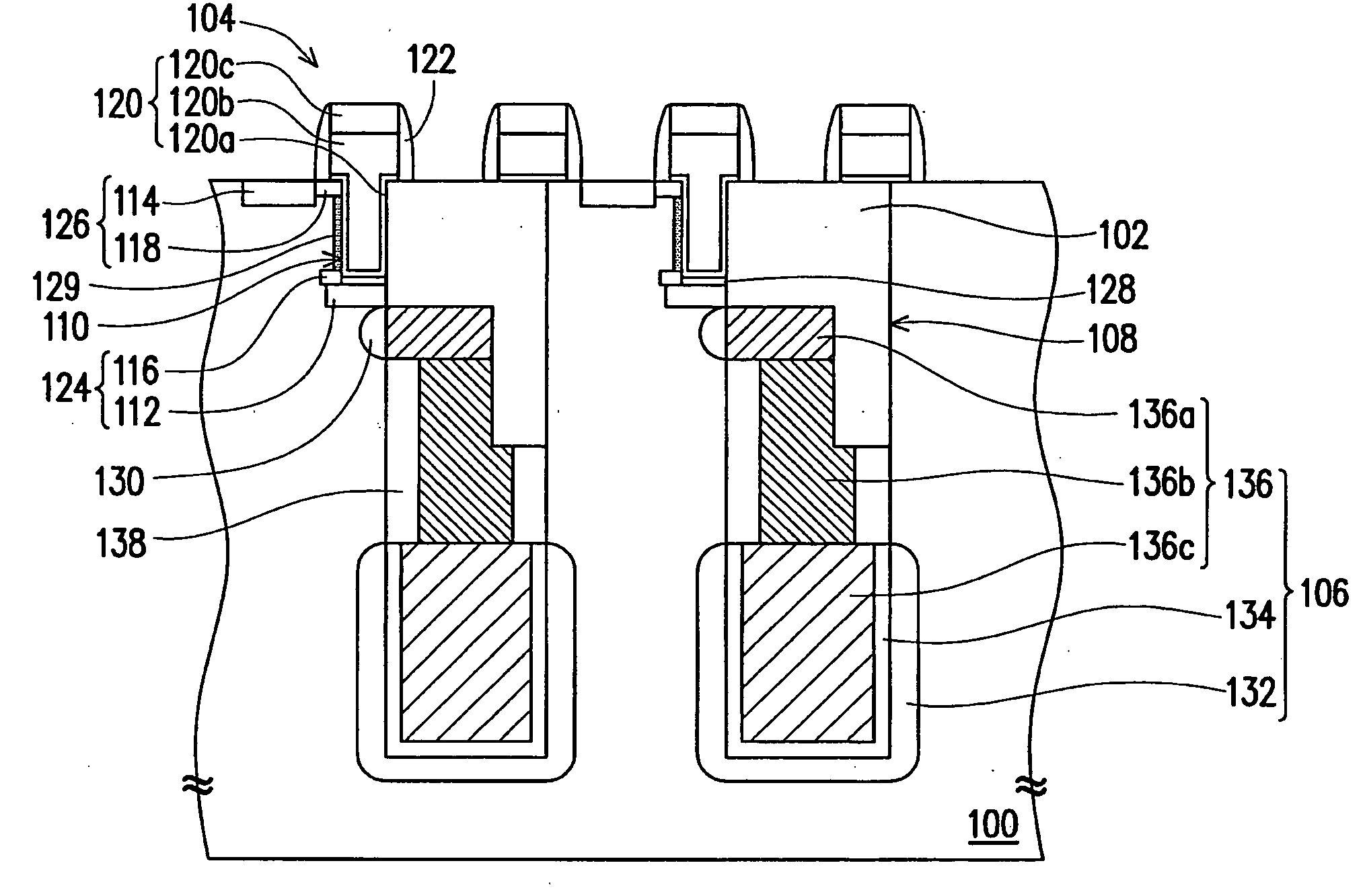
[0029]FIG. 1 is a cross-sectional view of a DRAM according to an embodiment of the present invention.

[0030]Referring to FIG. 1, the dynamic random access memory (DRAM) includes a substrate 100, an isolation structure 102, a buried strap 130, a vertical transistor 104 and a deep trench capacitor 106. The substrate 100 may be a silicon substrate. A deep trench 108 and a trench 110 are disposed in the substrate 100. The deep trench 108 is located on one side of the trench 110, and has a depth greater than that of the trench 110. The isolation structure 102 is disposed on the deep trench capacitor 106 to define an active region. The isolation structure 102 may be a shallow trench isolation structure, and...


PUM


Abstract

A dynamic random access memory (DRAM) is provided. The DRAM comprises a substrate, a vertical transistor, a deep trench capacitor and a buried strap. The substrate has a trench and a deep trench located on one side of the trench thereon. The vertical transistor is disposed in the trench, a portion of which is disposed on the substrate. The deep trench capacitor is disposed in the deep trench, and comprises a bottom electrode, a capacitor dielectric layer and a top electrode. The vertical transistor comprises a gate structure disposed in the trench and above the substrate, a first doped region disposed in the substrate on sidewalls and bottom of the trench, and a second doped region disposed in the substrate on top of the trench. The buried strap is disposed in the substrate below the vertical transistor, and is adjoined to the first doped region and the top electrode.

Description

CROSS-REFERENCE TO RELATED APPLICATION[0001]This application claims the priority benefit of Taiwan application serial no. 96118502, filed on May 24, 2007. All disclosure of the Taiwan application is incorporated herein by reference.BACKGROUND OF THE INVENTION[0002]1. Field of the Invention[0003]The present invention relates to a dynamic random access memory structure and a manufacturing method thereof. More particularly, the present invention relates to a dynamic random access memory structure having a vertical transistor and a deep trench capacitor and a manufacturing method thereof.[0004]2. Description of Related Art[0005]In the semiconductor industry, the dynamic random access memory (DRAM) is an important integrated circuit under constant studies and development. A DRAM cell generally includes a transistor and a capacitor controlled by the transistor. Presently, a structure of deep trench capacitor is developed in the DRAM industry, by which a capacitor is fabricated in the subs...

Claims


Application Information

Patent Timeline
Patent Type & Authority Applications(United States)
IPC IPC(8): H01L27/108H01L21/8242
CPCH01L27/10841H01L27/10867H10B12/395H10B12/0385
Inventor LIU, SHIH-WEN
Owner NAN YA TECH
Why Eureka
Try Eureka