METHOD OF MANUFACTURING ZnO-BASED THIN FILM TRANSISTOR

a thin film transistor and zno-based technology, applied in the direction of semiconductor devices, basic electric elements, electrical apparatus, etc., can solve the problems of increasing the carrier concentration, affecting the physical and electrical properties of the zno-based semiconductor film, etc., to reduce the carrier concentration, reduce the carrier concentration in the channel layer, and reduce the carrier concentration

Inactive Publication Date: 2008-12-04
SAMSUNG ELECTRONICS CO LTD
View PDF11 Cites 297 Cited by
  • Summary
  • Abstract
  • Description
  • Claims
  • Application Information

AI Technical Summary

Benefits of technology

[0009]According to one embodiment, there is provided a method of manufacturing a thin film transistor (TFT), the method comprising: forming a channel layer comprising ZnO on a substrate; forming an oxide layer comprising unstable or incompletely bonded oxygen on the channel layer; and annealing the channel layer and the oxide layer, wherein the annealing of the channel layer and the oxide layer allows oxygen of the oxide layer to be introduced to the channel layer, thereby inducing an interfacial reaction between the channel layer and the oxide layer and reducing carrier concentration in the channel layer.
[0010]According to another embodiment, there is provided a method of manufacturing a TFT, the method comprising: forming a channel layer comprising ZnO on a substrate; forming a conductive material layer on the channel layer; patterning the conductive material layer to form a source electrode and a drain electrode contacting both sides of the channel layer; forming an oxide passivation layer comprising unstable or incompletely bonded oxygen on the channel layer, the source electrode, and the drain electrode; and annealing the channel layer and the passivation layer to introduce oxygen of the passivation layer to the channel layer, thereby inducing an interfacial reaction between the channel layer and the passivation layer, and reducing carrier concentration in the channel layer.
[0011]According to another embodiment, there is provided a method of manufacturing a TFT, the method comprising: forming a channel layer comprising ZnO on a substrate; forming an oxide material layer containing unstable or incompletely bonded oxygen on the channel layer; patterning the oxide material layer to form an etch stop layer covering a middle portion of the channel layer and exposing both sides of the channel layer; forming a conductive material layer on the channel layer and the etch stop layer; patterning the conductive material layer to form a source electrode and a drain electrode contacting both the sides of the channel layer; forming a passivation layer covering the source electrode, the drain electrode, and a portion of the etch stop layer between the source electrode and the drain electrode; and annealing the channel layer and the oxide material layer to introduce oxygen of the etch stop layer to the channel layer, thereby inducing an interfacial reaction between the channel layer and the etch stop layer, and reducing carrier concentration in the channel layer.

Problems solved by technology

However, carrier concentration in the ZnO-based semiconductor film is sensitive to changes in oxygen concentration, and the physical and electrical properties of the ZnO-based semiconductor film are greatly affected by both thermal and chemical treatments.
When a TFT comprising a ZnO-based semiconductor film is manufactured, the ZnO-based semiconductor film is exposed to high-energy plasma and is thus subject to plasma-induced damage and thermal damage, thereby increasing the carrier concentration.
The abnormal increase in the carrier concentration shifts the threshold voltage of the ZnO-based TFT to a larger negative voltage, such that a large leakage current flows between a source electrode and a drain electrode even when the gate voltage is 0 V. The leakage current is a critical problem in cases where the ZnO-based TFT is a back channel etch (BCE) TFT in which a SiNx passivation layer is formed on both the source and the drain electrodes, and where the ZnO-based TFT is an etch stopper TFT in which a channel layer is protected by an etch stopper and both the source and the drain electrodes are formed by etching.

Method used


Image

  • METHOD OF MANUFACTURING ZnO-BASED THIN FILM TRANSISTOR
  • METHOD OF MANUFACTURING ZnO-BASED THIN FILM TRANSISTOR
  • METHOD OF MANUFACTURING ZnO-BASED THIN FILM TRANSISTOR

Examples


Embodiment Construction

[0032]The present invention will now be described more fully with reference to the accompanying drawings, in which exemplary embodiments of the invention are shown.

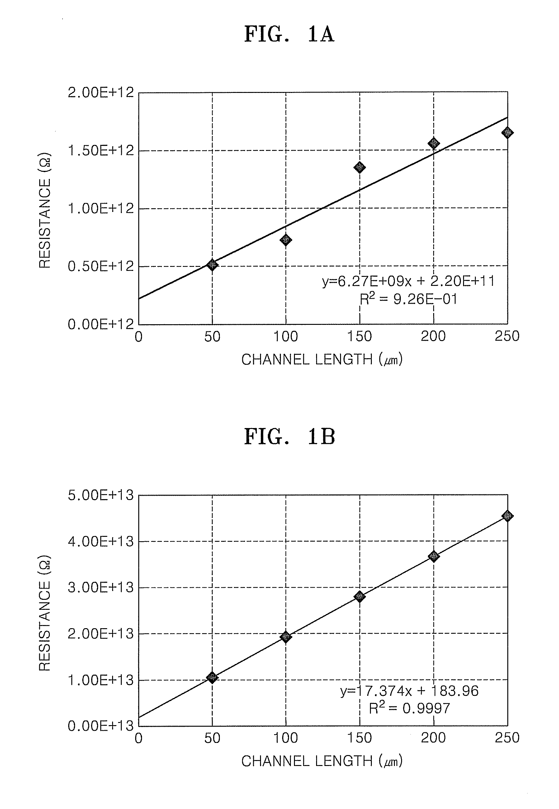
[0033]FIGS. 1A and 1B are graphs illustrating the electrical properties of a patterned ZnO-based semiconductor channel layer, specifically, a gallium-indium-zinc-oxide (GIZO) channel layer, before and after annealing.

[0034]Referring to FIG. 1A, the GIZO channel layer, before annealing, has a conductivity of 1.47×10⁻⁸ (Siemens per centimeter) (S / cm). Referring to FIG. 1B, the GIZO channel layer, after annealing, is thermally unstable and has a conductivity of 1.71×100 S / cm.

[0035]The thermal instability and increase in electrical conductivity after annealing, results from the collision of high-energy plasma ions released when the source and the drain electrodes are formed by patterning, and from a subsequent increase in carrier concentration in the channel layer. The increase in the carrier concentration causes the thin fil...


PUM


Abstract

A ZnO-based thin film transistor (TFT) is provided herein. Also provided is a method for manufacturing the TFT. The ZnO-based TFT is very sensitive to the oxygen concentration present in a channel layer. In order to prevent damage to a channel layer of a bottom gate TFT, and to avoid a deep negative threshold voltage resulting from damage to the channel layer, the method for manufacturing the ZnO-based TFT comprises formation of an etch stop layer or a passivation layer comprising unstable or incompletely bonded oxygen, and annealing the layers to induce an interfacial reaction between the oxide layer and the channel layer and to reduce the carrier concentration.

Description

[0001]This application claims priority to Korean Patent Application No. 10-2007-0051560, filed on May 28, 2007, and all the benefits accruing therefrom under 35 U.S.C. § 119, the contents of which is incorporated herein in their entirety by reference.BACKGROUND OF THE INVENTION[0002]1. Field of the Invention[0003]The present disclosure relates to an oxide semiconductor thin film and a method of manufacturing a thin film transistor (TFT) using the same, and more particularly, to a semiconductor thin film comprising ZnO and a method of manufacturing a TFT using the same.[0004]2. Description of the Related Art[0005]Thin film transistors (TFTs) using a semiconductor thin film are applied in various fields, and are often used as active devices for flat panel displays. Specifically, oxide semiconductor films, particularly, semiconductor films comprising ZnO, for example an amorphous gallium-indium-zinc-oxide (GIZO) semiconductor film, can be processed at low temperatures and can be easily...

Claims


Application Information

Patent Timeline
Patent Type & Authority Applications(United States)
IPC IPC(8): H01L21/00H01L21/84
CPCH01L29/7869
Inventor SON, KYOUNG-SEOKLEE, SANG-YOONRYU, MYUNG-KWANKIM, TAE-SANGKWON, JANG-YEONPARK, KYUNG-BAEJUNG, JI-SIM
Owner SAMSUNG ELECTRONICS CO LTD
Why Eureka
Try Eureka