Single Crystal Manufacturing Method

a manufacturing method and single crystal technology, applied in the direction of crystal growth process polycrystalline material growth, etc., can solve the problems of increasing the weight of raw materials, and reducing the yield of silicon single crystal ingots, etc., to achieve good crystal shape

Active Publication Date: 2008-12-11
SILTRONIC AG
View PDF18 Cites 13 Cited by
  • Summary
  • Abstract
  • Description
  • Claims
  • Application Information

AI Technical Summary

Benefits of technology

[0026]It is an object of the present invention to provide a manufacturing method for single crystals, which stably pulls a single crystal completely free from dislocations, and with a good crystal shape. These and other objects are achieved by a manufacturing method for single crystals by single CZ crystal growth while applying a horizontal magnetic field to the raw material melt, wherein the magnetic field center is positioned lower than the liquid surface of the melt by more than 50 mm and at a distance equal to or less than a depth L from the liquid surface of the melt remaining in the crucible during pulling of the constant diameter part of the single crystal. In a preferred mode, the magnetic field center is set at a position between 50 mm to 90 mm from the liquid surface.

Problems solved by technology

As the diameter of the silicon single crystal increases, an increasingly large weight of raw material is required.
As a result, the diameter of the pulled silicon single crystal is periodically changed in the longitudinal direction, and can become smaller than the predetermined diameter, which causes yield reduction in the manufacture of the silicon single crystal ingots.
However, increasing the target diameter also reduces yield due to the increased diameter elsewhere, and thus this method cannot prevent reduced yield.
However, under such crystal pulling conditions, as a unique phenomenon associated with use of a horizontal magnetic field, part of the molten silicon surface solidifies in low-temperature regions of the silicon melt surface, the solidified silicon ultimately contacts the single crystal during pulling, and causes dislocations in the pulled crystal.
Therefore, all the crystal pulling conditions described above cause yield reduction in silicon single crystal manufacture.
However, when the magnetic field center position is too close to the liquid surface of the silicon melt like the case of FIG. 6A, the phenomenon of unstable silicon melt flow appears.
Particularly when the weight of the silicon melt is large, this phenomenon becomes serious.
Also in the case in which the distance between the liquid surface of the silicon melt and the magnetic center position is large, the convection of the silicon melt also becomes unstable, and a similar problem occurs.
Therefore, stability of the magnetic field strength applied to the molten silicon cannot be obtained.

Method used


Image

  • Single Crystal Manufacturing Method
  • Single Crystal Manufacturing Method
  • Single Crystal Manufacturing Method

Examples


examples

[0056]Hereinafter, examples of the present invention will be described.

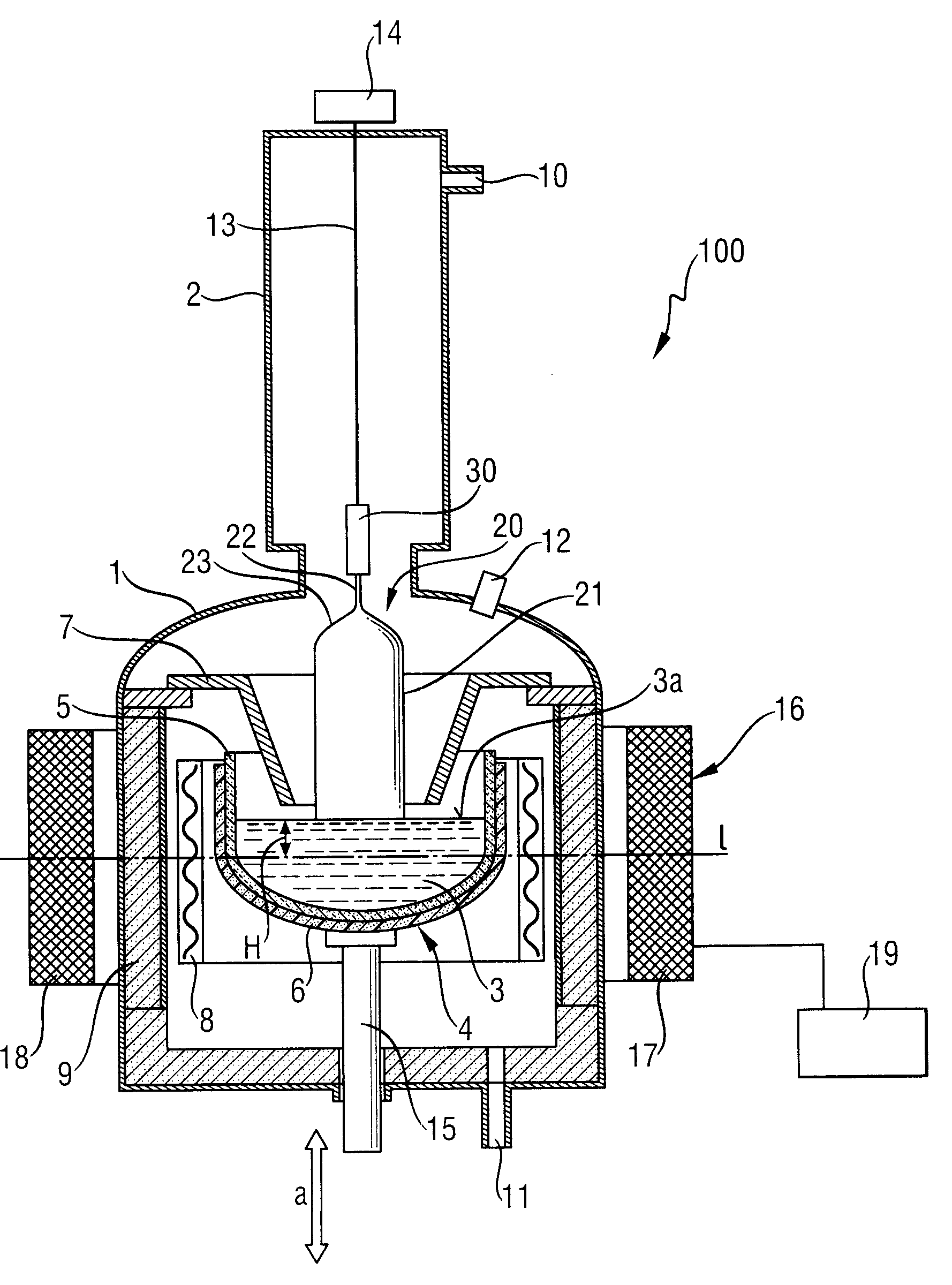
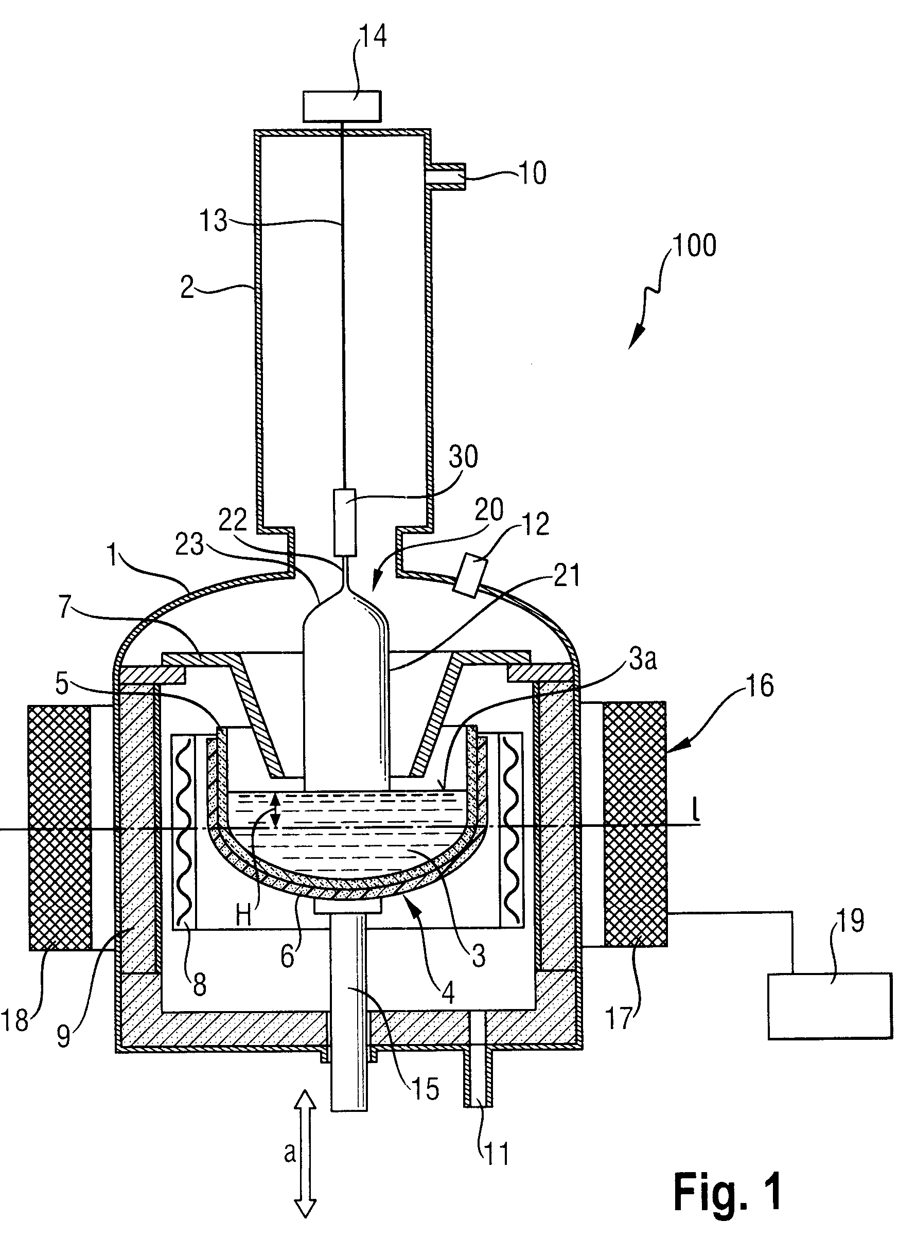
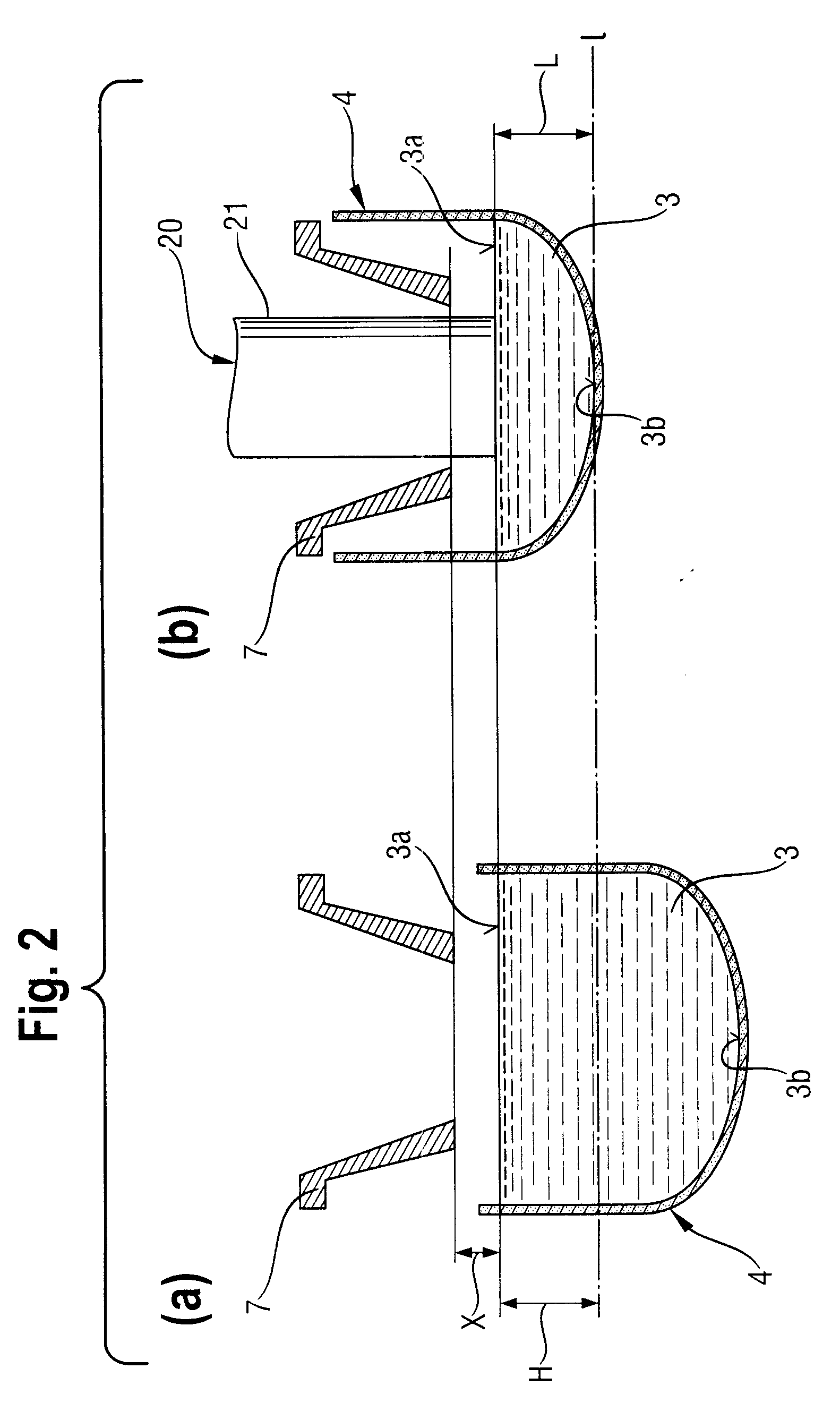
[0057]Pulling of a silicon single crystal was carried out by the above described embodiment by using the single crystal manufacturing apparatus 100 of FIG. 1. Specifically, when the magnetic field center distance H was 60, 70, and 90 mm, pulling of silicon single crystal ingots was carried out, respectively, so that the number of the ingots were: n=4 when H=60 mm, n=4 when H=70 mm, and n=3 when H=90 mm (Examples 1 to 3).

[0058]In the present examples, the diameter of the quartz crucible 5 was 28 inches (700 mm), based on specifications such as desired resistivity, in order to manufacture a silicon single crystal ingot in which constant diameter length is 1000 mm, and the crystal diameter of the constant diameter part is 306 mm, to take into consideration a grinding allowance in subsequent cylindrical grinding so that the crystal diameter of the complete product would be 300. 220 kg of block polycrystalline silicon...


PUM

PropertyMeasurementUnit
diameteraaaaaaaaaa
diameteraaaaaaaaaa
sizesaaaaaaaaaa

Abstract

Single crystalline ingots can be stably pulled free from dislocation and with a good crystal shape by actuating a crystal driving unit so as to immerse a seed crystal in a silicon melt, and controlling the crystal driving unit and a crucible driving unit under predetermined conditions so as to pull the seed crystal. During pulling, a horizontal magnetic field positioning device applies a magnetic field in the horizontal direction to the inside of the silicon melt, fixing the magnetic field axis at a constant position from the liquid surface of the melt. Positional adjustment of the vertical position of the horizontal magnetic field is performed in advance by a magnetic field position adjusting device, and the magnetic field axis of the applied field is fixed at a constant distance lower than the liquid surface of the melt by more than 50 mm and at the same level or higher than a depth L from the melt surface at the point of tail-in.

Description

BACKGROUND OF THE INVENTION[0001]1. Field of the Invention[0002]The present invention relates to a manufacturing method for single crystals using the Czochralski process (hereinafter, referred to as the CZ process) and in particular to a method for manufacturing silicon single crystals by using the MCZ process in which a horizontal magnetic field is applied to a silicon melt during pulling of the single crystal.[0003]2. Background Art[0004]Recently, high integration and fine structurization of elements has advanced in semiconductor devices, and accordingly improvement in the quality of the silicon single crystal substrate material has been increasingly demanded. Particularly, reduction of Grown-in defects introduced during pulling of the silicon single crystal is strongly needed. Many pulling methods for reducing these defects, for example methods for pulling a silicon single crystal in an N region, have been proposed.[0005]In addition to improving the yield of semiconductor devices...

Claims


Application Information

Patent Timeline
Patent Type & Authority Applications(United States)
IPC IPC(8): C30B15/00
CPCC30B15/305C30B29/06C30B15/00
Inventor OHKUBO, MASAMICHI
Owner SILTRONIC AG
Why Eureka
Try Eureka