On chip timing adjustment in multi-channel fast data transfer

a multi-channel, data transfer technology, applied in pulse manipulation, pulse technique, instruments, etc., can solve the problems of large propagation delay time difference, timing uncertainty, driver and receiver chip procession variance,

Inactive Publication Date: 2008-12-11
MARVELL ASIA PTE LTD
View PDF31 Cites 17 Cited by
  • Summary
  • Abstract
  • Description
  • Claims
  • Application Information

AI Technical Summary

Problems solved by technology

The following factors can cause timing uncertainty.
The first factor that can cause timing uncertainty is driver and receiver chip procession variance.
A small portion of geometric variance in a small sized device would cause a relatively big propagation delay time difference.
The second factor that can cause timing uncertainty is noise.
The wide bandwidth results in more noise and large timing jitter on the transition edges since the noise rms value is proportional to the square root of the bandwidth.
A third factor that can cause timing uncertainty is the difference of the length of the microstrip lines on a printed circuit board (PCB) between the driver and the receiver.
However, the signal speed in a microstrip line depends on the dielectric constant of the PCB and is much slower than the speed in vacuum or in air.
This causes considerable timing differences for different lengths of microstrip lines in a PCB.
In an actual PCB layout, it is not feasible to keep all microstrip line channel lengths the same length.
According to the problems describe above, even if the chips of a driver or receiver have excellent stand-alone timing performances (and good jitter budgets) when they are mounted on the PCB, serious timing problems could still exist because of driver and receiver chip processing variances, noise, and / or different microstrip line channel lengths.

Method used


Image

  • On chip timing adjustment in multi-channel fast data transfer
  • On chip timing adjustment in multi-channel fast data transfer
  • On chip timing adjustment in multi-channel fast data transfer

Examples


Embodiment Construction

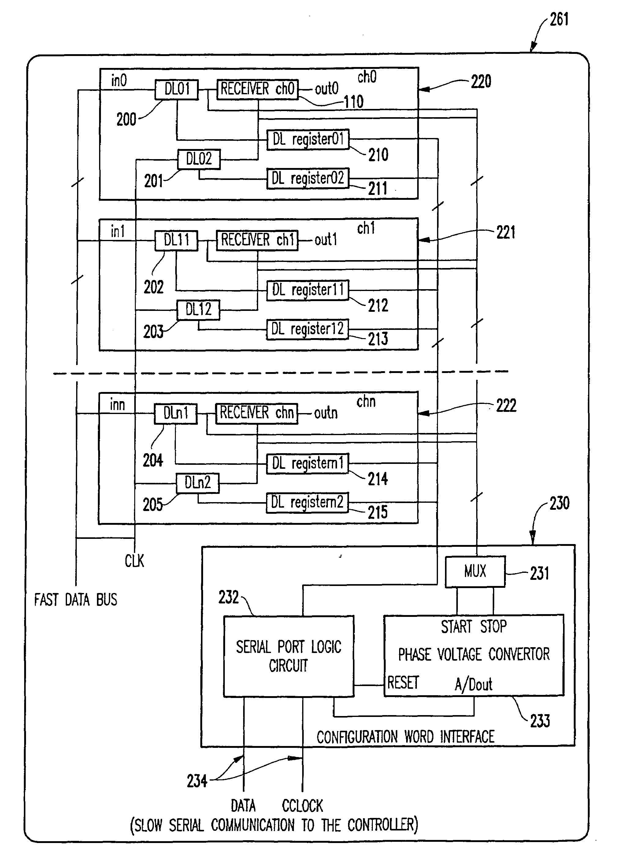
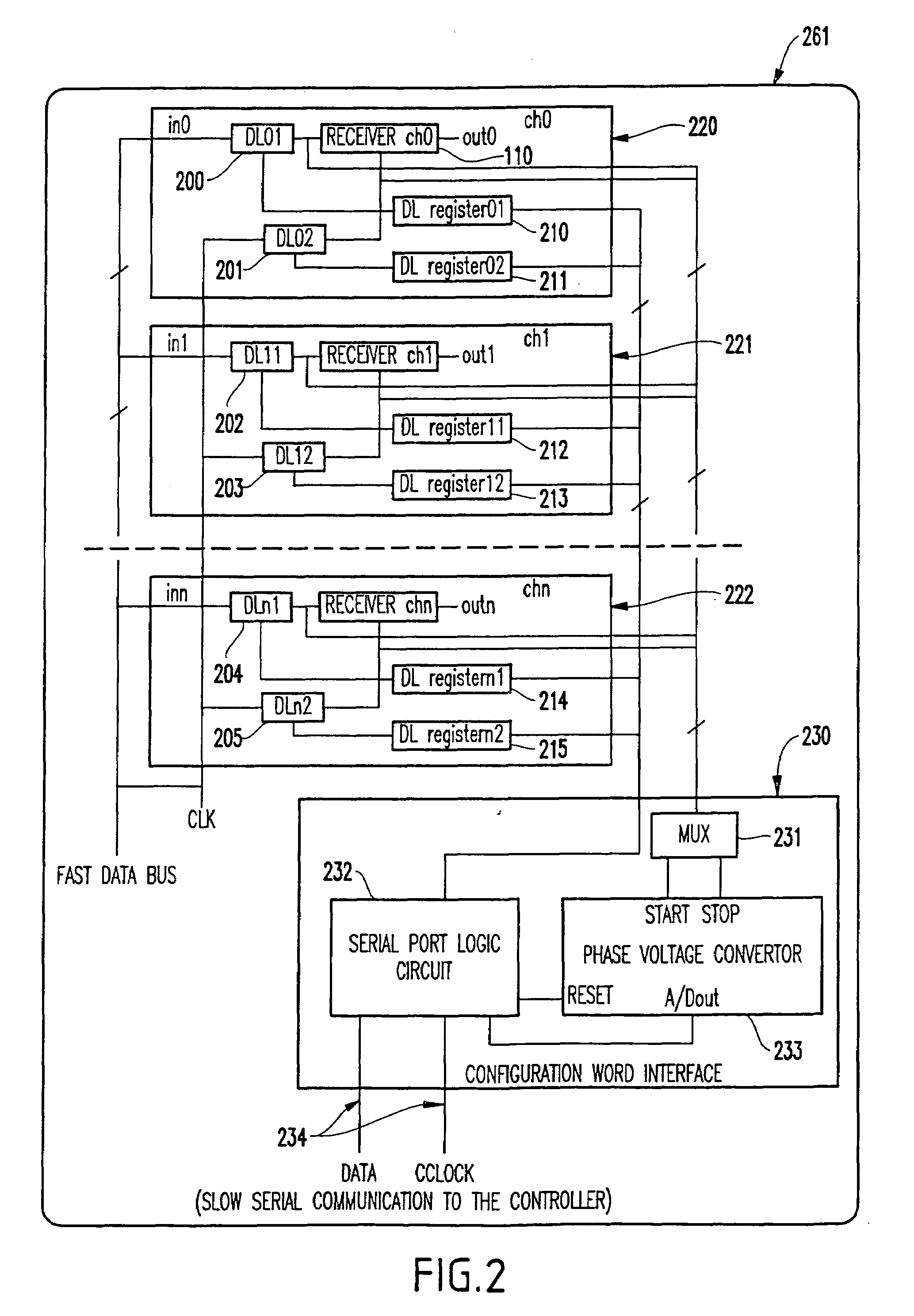
[0028]As mentioned above, even if the chips of a driver or receiver have excellent stand-alone timing performances (and good jitter budgets) when they are mounted on the PCB, serious timing problems could still exist because of driver and receiver chip processing variances, noise, and / or different microstrip line channel lengths. The invention described below overcomes these problems with a novel chip timing adjustment structure which is implemented by programmable delay units and configuration word settings. Thus, the invention provides a solution of “on-chip” timing adjustment using programmable delay units and configuration word settings.

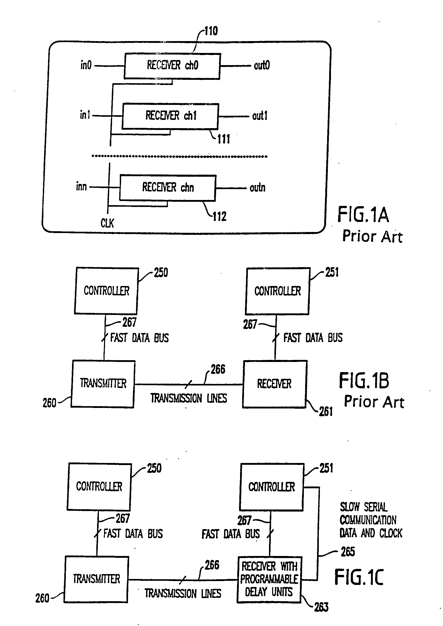
[0029]Referring now to FIG. 1(a), a system block diagram is shown. More specifically, FIG. 1(a) shows the block diagram of a receiver having N parallel channels 110-112. Good timing results are required, not only for the input bit signal and clock of each channel, but also among the outputs of all channels. Due to the noise jitters, procession va...


PUM


Abstract

A method and structure for an apparatus for maintaining signal integrity between integrated circuits residing on a printed circuit board. The apparatus has adjustable delay circuitry within the circuits and the adjustable delay circuitry adjusts the timing of signals processed within the circuit. A phase monitor connects to the circuits. The phase monitor detects phase differences between signals output by the circuits. A controller connected to the delay circuitry, the phase monitor, and the controller adjust the delay circuitry to compensate for the phase differences.

Description

CROSS-REFERENCE TO RELATED APPLICATIONS [0001]This application is a continuation of U.S. application Ser. No. 11 / 232,675 filed Sep. 22, 2005, which is a division of U.S. application Ser. No. 10 / 063,394 filed on Apr. 18, 2002, the complete disclosures of which, in there entirety, are herein incorporated by reference.BACKGROUND OF THE INVENTION [0002]1. Field of the Invention[0003]The present invention generally relates to chip timing adjustment and more particularly to a chip timing adjustment structure which is implemented by programmable delay units and configuration word settings.[0004]2. Description of the Related Art[0005]As the Baud rate increases, the timing performance of fast digital transfer systems becomes more and more critical. This is especially true for multi-channel, fast digital transfer systems because the timing concern in this kind of system is not only for data and clock information, but also for information between channels.[0006]The following factors can cause ...

Claims


Application Information

Patent Timeline
Patent Type & Authority Applications(United States)
IPC IPC(8): H03L7/06H03K5/01H03K7/00G06F11/00H03L7/00
CPCG06F11/00H03L7/00
Inventor FENG, KAI DI
Owner MARVELL ASIA PTE LTD
Why Eureka
Try Eureka