Semiconductor memory device

Inactive Publication Date: 2008-12-11
FUJITSU LTD
View PDF7 Cites 2 Cited by
  • Summary
  • Abstract
  • Description
  • Claims
  • Application Information

AI Technical Summary

Benefits of technology

[0013]However, when the above transistor configuration disclosed in Patent Document 1 is applied to a memory cell, the drive line of the memory cell is selected by the column line. Therefore, in an existing bit cell, Pwells and Nwells are separated in parallel rows. Thus, when a column selection signal is used, the separation direction of the Pwell and Nwell needs to be changed to the vertical (column) direction, so that the configuration of the bit cell needs to be modified. The existing bit cell is optimized with the operating speed and integration degree taken into consideration, so that the modification of the bit cell greatly influences its performance.
[0015]The present invention has been made to solve the above problems, and an 5 object thereof is to provide a semiconductor memory device capable of increasing its drive capability at operating time while reducing a leak current at standby time without the need to make a significant change to the design of an existing semiconductor memory device.

Problems solved by technology

Therefore, the drive capability of an NMOS required at the data read time is low, Further, in an RAM including a large number of row lines like a large capacity memory, the load capacitance of the bit lines (BL, BLX) to be driven for the internal NMOS is large, so that there is a possibility that access time for the RAM may become longer to degrade system performance.
The capacity of a cache memory mounted on a high-performance processor increases as the generation progresses, and the power consumption of the cache memory occupies the majority of the power consumption (especially standby power consumption) in a chip.
Since the drive capability of the transistor in a memory cell is lower than that of a commonly-used transistor as described above, the time required for generating a potential difference for allowing the sense amplifier to operate, that is, the time required for recognizing “High” or “Low” becomes longer with the result that the memory access time becomes longer, which may restrict the chip performance.

Method used


Image

  • Semiconductor memory device
  • Semiconductor memory device
  • Semiconductor memory device

Examples


Embodiment Construction

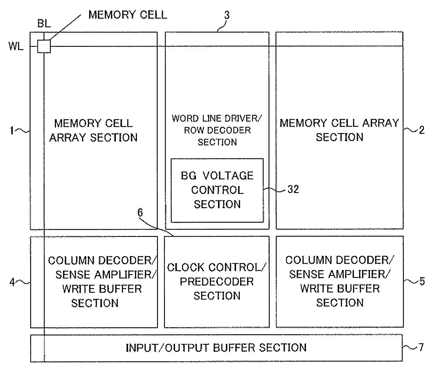
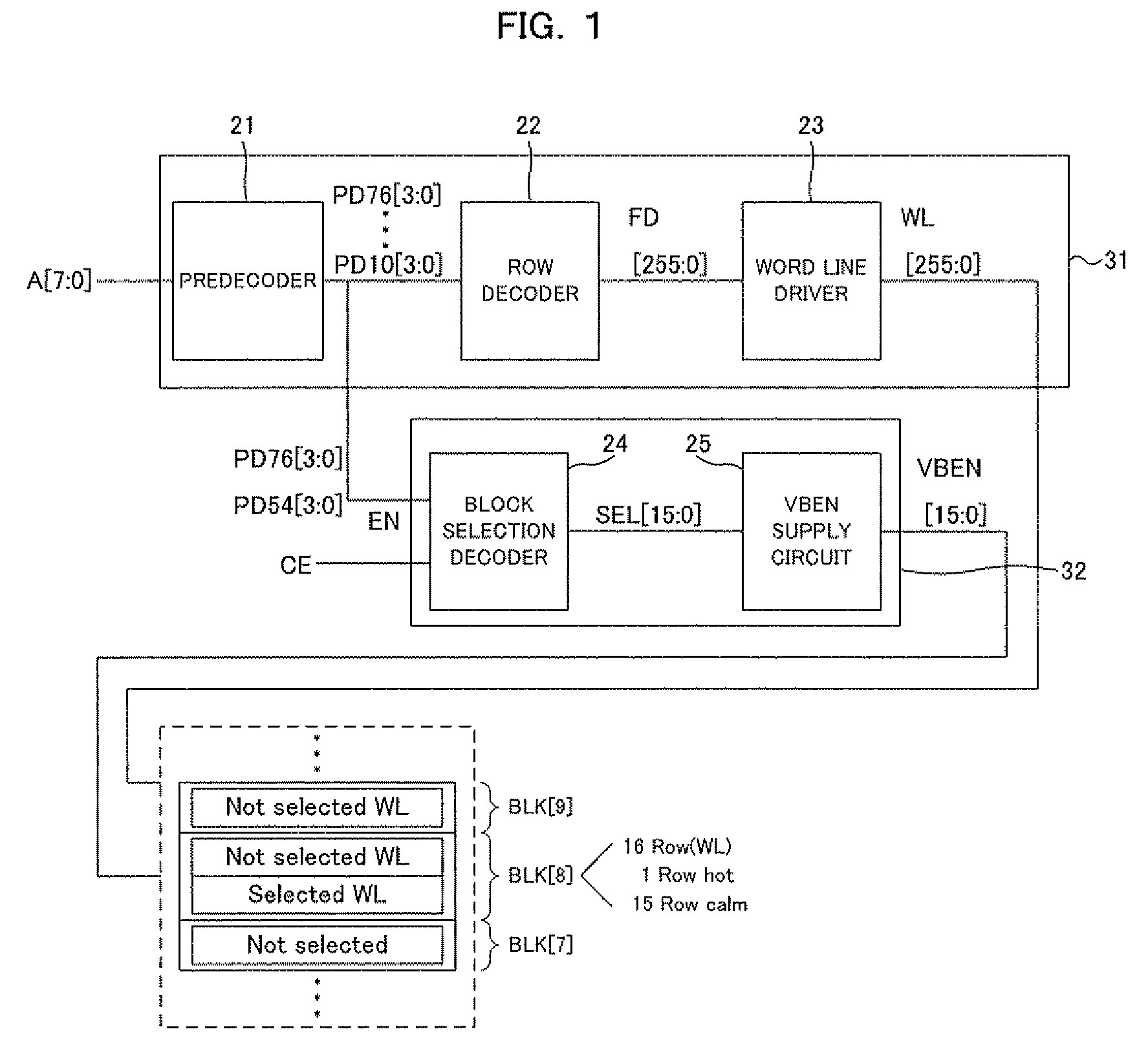
[0025]An embodiment of the present invention will be described below by referring to the accompanying drawings.

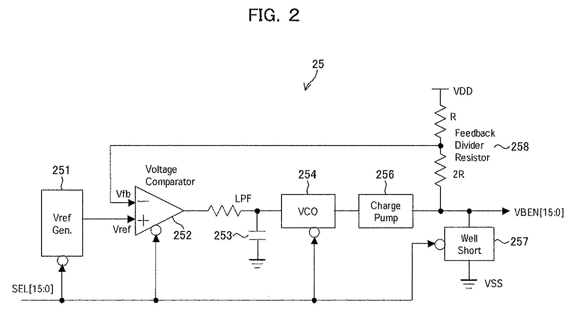
[0026]In an embodiment of the present invention, a BG terminal of a transistor constituting a memory cell is disconnected from a VDD or VSS power supply so as to change the potential of the BG terminal depending on selection / nonselection of a memory cell. This configuration allows the threshold voltage of the transistor in a selected memory cell to be reduced to thereby increase drive capability while allowing the threshold voltage of the transistor in a nonselected memory cell to be increased to thereby suppress a leak current. The above configuration can be achieved without the need to make a significant change to the design of an existing semiconductor memory device.

[0027]In the memory cell array, wells of the same type are sequentially arranged in the row direction for convenience of layout. Therefore, when a signal for selecting a row is used as an EN signal to apply a...


PUM


Abstract

To provide a semiconductor memory device capable of increasing its drive capability at operating time while reducing a leak current at standby time without the s need to make a significant change to the design of an existing semiconductor memory device a semiconductor memory device having a memory cell comprises: a latch section that includes a transistor having a back gate to which a back gate voltage is supplied; a memory cell that includes a transfer gate constituting the memory cell the transfer gate being subjected to switching control by a word line signal and having a lo back gate to which a back gate voltage is supplied; and a back gate voltage control circuit that controls the back gate voltage based on an address signal.

Description

TECHNICAL FIELD[0001]The present invention relates to a semiconductor memory device that performs a memory access operation by using word (row) lines and bit (column) lines.BACKGROUND ART[0002]FIG. 7 is a block diagram showing a configuration of a RAM macro of a semiconductor memory device by taking “2 kw 1RW RAM (8 col / 1 bit system)” as an example. As shown in FIG. 7, the RAM macro is divided into memory cell array sections 1 and 2, a word line (WL) driver / row decoder section 3, a column decoder / sense amplifier (sense amp) / write buffer sections 4 and 5, and a clock control / predecoder section 6, which are connected to an input / output buffer section 7.[0003]FIG. 8 is a circuit diagram for explaining a drive line (word line) that drives a memory cell. One memory cell 10 includes two transfer gates 11 and 12 which are data input / output control transistors for controlling input / output of data on its input and output sides and a latch section 14 provided between the two transfer gates 11...

Claims


Application Information

Patent Timeline
IPC IPC(8): G11C7/00G11C8/00G11C5/14
CPCG11C5/146G11C8/10G11C11/412G11C11/413
Inventor HARADA, AKIHIKO
Owner FUJITSU LTD
Why Eureka
Try Eureka