Nitride semiconductor device and method for producing nitride semiconductor device

a technology of nitride and semiconductors, applied in the direction of semiconductor devices, basic electric elements, electrical apparatus, etc., can solve the problems of high silicon device speed and difficulty in satisfying market needs

Inactive Publication Date: 2008-12-18
ROHM CO LTD
View PDF3 Cites 23 Cited by
  • Summary
  • Abstract
  • Description
  • Claims
  • Application Information

AI Technical Summary

Benefits of technology

[0039]FIG. 6 is a diagram showing results of gate withstand voltage measurement of field effect transistors of Example 2 and Compar

Problems solved by technology

However, from theoretical limitations of the silicon semiconductor, high withstand voltage, low resistance, and high

Method used


Image

  • Nitride semiconductor device and method for producing nitride semiconductor device
  • Nitride semiconductor device and method for producing nitride semiconductor device
  • Nitride semiconductor device and method for producing nitride semiconductor device

Examples


example 1

[0085]On a substrate, a GaN nitride semiconductor laminated structure formed of an npn laminated structure in which an n type GaN layer (first layer), a p type GaN layer (second layer), and an n type GaN layer (third layer) were laminated by MOCVD was manufactured. Then, in this GaN nitride semiconductor laminated structure, from the surface of the n type GaN layer (third layer), a trench which penetrates the p type GaN layer (second layer) and reaches the middle of the n type GaN layer (first layer) was formed. Then, on the bottom surface of this trench, a drain electrode (Ti / Al laminated structure) was formed, and on the top surface of the n type GaN layer (third layer), a source electrode (Ti / Al laminated structure) was formed. Then, between the source and the drain, an insulating film (film thickness: 100 angstroms) made of SiN was formed so as to cover the bottom surface and the side surfaces of the trench and the top surface of the n type GaN layer (third layer) (see FIG. 4).

example 2

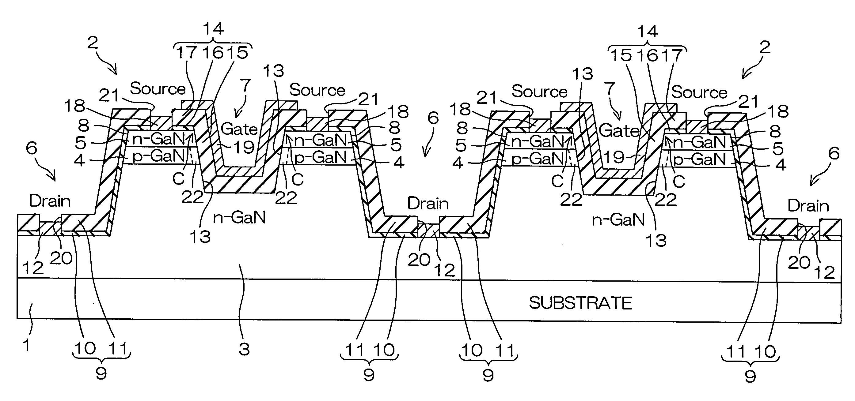
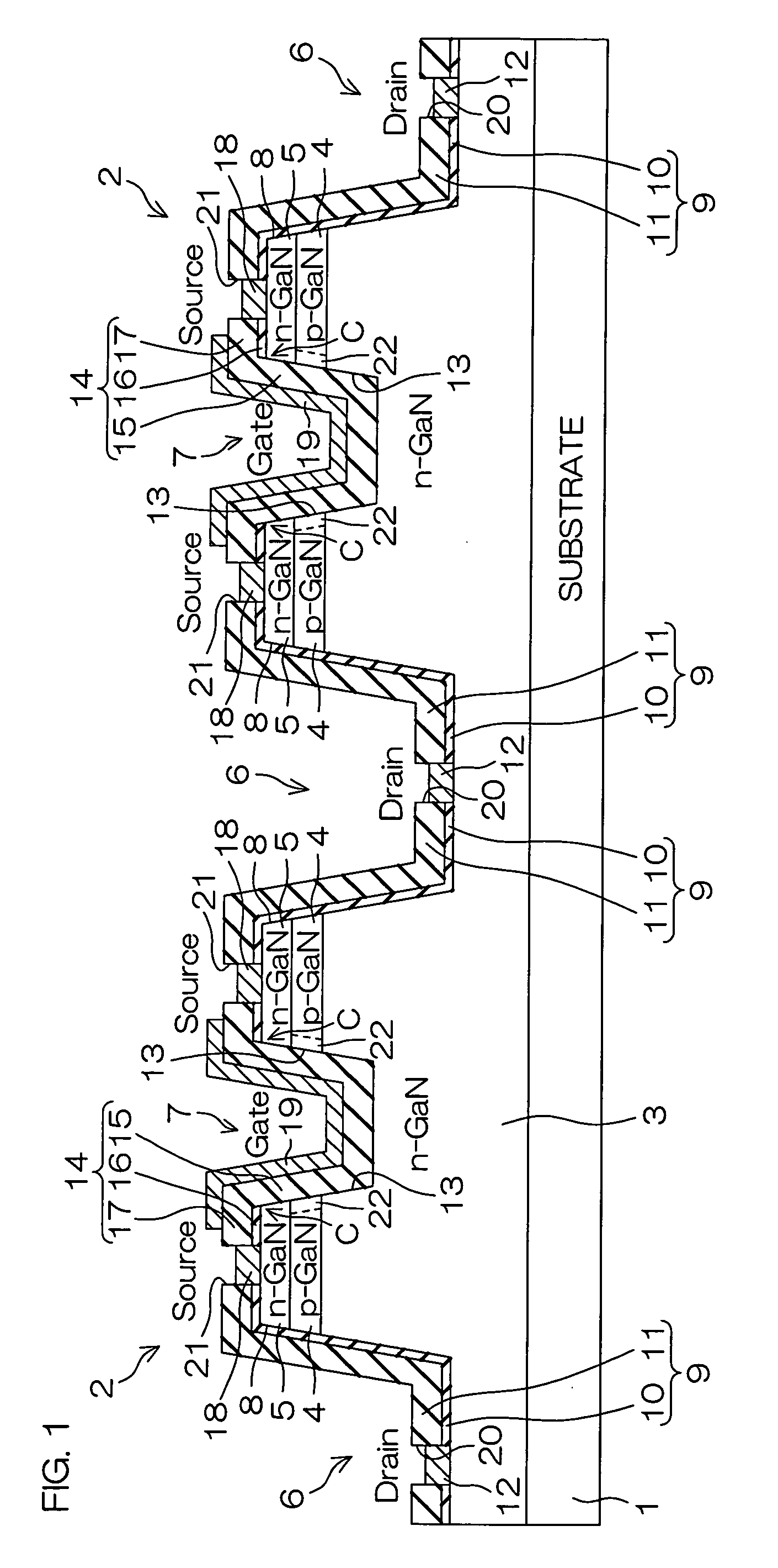
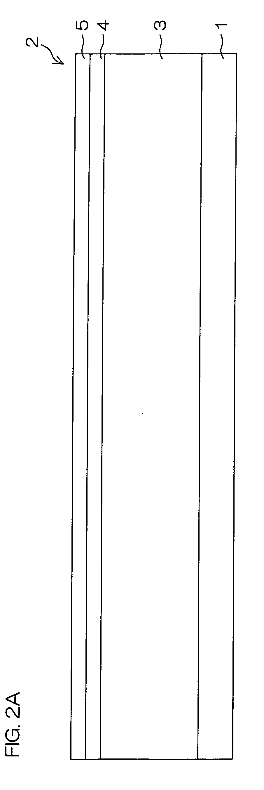
[0088]A field effect transistor having the structure shown in FIG. 1 was manufactured according to the production steps shown in FIG. 2A through FIG. 2H.


PUM


Abstract

A nitride semiconductor device of the present invention includes: a nitride semiconductor laminated structure comprising an n type first layer, a second layer containing a p type dopant laminated on the first layer, and an n type third layer laminated on the second layer, each layer of the nitride semiconductor laminated structure made of a group III nitride semiconductor, and the nitride semiconductor laminated structure formed with a first trench and a second trench, the first trench penetrating the second layer from the third layer and reaching at least the first layer, and the second trench having a side wall extending from the first, second, to third layers and being different from the first trench; a surface insulating film containing at least silicon nitride formed such that the surface insulating film covers the surface of the first trench; a gate insulating film formed on the side wall of the second trench such that the gate insulating film extends over the first, second, and third layers; and a gate electrode formed such that the gate electrode is opposed to the side wall of the second trench with the gate insulating film sandwiched between the gate electrode and the side wall.

Description

BACKGROUND OF THE INVENTION[0001]1. Field of the Invention[0002]The present invention relates to a nitride semiconductor device using a Group III nitride semiconductor and a manufacturing method thereof.[0003]2. Description of Related Art[0004]Conventionally, a power device using a silicon semiconductor is used for a power amplifier circuit, a power supply circuit, a motor drive circuit, or the like.[0005]However, from theoretical limitations of the silicon semiconductor, high withstand voltage, low resistance, and high speed of the silicon device have nearly reached their limits, which leads to difficulties in satisfying market needs.[0006]Therefore, consideration has been given to the development of a nitride semiconductor device having characteristics such as high withstand voltage, high-temperature operation, a large current density, high-speed switching, low on-resistance, and the like.[0007]FIG. 7 is a diagrammatic sectional view for describing the structure of a conventional ...

Claims


Application Information

Patent Timeline
IPC IPC(8): H01L29/20H01L21/20
CPCH01L29/2003H01L29/41766H01L29/66734H01L29/7809H01L29/7813
Inventor OTAKE, HIROTAKA
Owner ROHM CO LTD
Why Eureka
Try Eureka