Semiconductor Radiation Detector Optimized for Detecting Visible Light

a radiation detector and semiconductor technology, applied in the field of semiconductor radiation detectors, can solve the problems of poor blue response of front illuminated novel mig detectors, and achieve the effects of improving the blue response of front illuminated devices, reducing the number of secondary charges, and reducing the size of the active area

Active Publication Date: 2008-12-25
AUROLA ARTTO
View PDF10 Cites 6 Cited by
  • Summary
  • Abstract
  • Description
  • Claims
  • Application Information

AI Technical Summary

Benefits of technology

[0011]The invention is based on the idea of removing the conducting back side layer from the MIG detector. It is realised that the secondary charges generated in the bulk layer can be collected inside the active area by channel stops instead of using a conductive backside layer for transporting them outside the active area. The collection of the secondary charges from the bulk layer inside the active area can be further improved by gaps in the MIG layer and by trench structures that are properly filled. It is also realised that a novel MIG detector can be front illuminated. The front illuminated novel MIG detector suffers, however, from poor blue response because of the following fact. The barrier layer forms a barrier for the signal charges between the MIG layer and the surface of the device. Blue light is absorbed mainly between this barrier and the front surface of the detector and thus a large portion of the signal charges generated by blue light is collected by the pixel doping and not by the MIG. By realising that such a barrier does not exist below the channel stops and that the channel stop area can be used as a radiation entry window and by further realising that the channel stops can be very thin and that the channel stop area can be very large in size, the blue response of a front illuminated device can be improved significantly. The large area of the channel stops reduces, however, the signal charge transporting potential gradient in the MIG layer under the channel stops. It is further realised that this potential gradient transporting the signal charges can be improved by a structured, i.e. by a discontinuous MIG layer. Another possibility is to alter the doping concentration in the barrier layer, in the MIG layer or in the bulk layer next to the MIG layer in order to improve the potential gradient transporting the signal charges. In the front illuminated detector the secondary charges that are generated in the bulk can be collected by the channel stops inside the active area, and / or by a substrate contact situated outside the active area on the front side of the detector, and / or by a substrate contact situated on the edge of the detector chip or on the backside of the detector chip.
[0012]The signal charges can be cleared using only a small voltage by a structure where there is in the barrier layer of the first conductivity type a doped region of the second conductivity type or a local reduction of the barrier layer net doping between the modified internal gate layer of second conductivity type and a pixel doping of second conductivity type or by a structure where there is a trench between the MIG layer doping and the front surface of the detector, and where a gate controls the flow of signal charges from the modified internal gate layer to the pixel doping or to the front surface of the detector through the doped region of second conductivity type, through the trench structure or through the local reduction of the barrier layer doping.
[0013]The separation of the signal charges and of the surface generated charges can be improved for instance by a doped region of the second conductivity type situated between the barrier layer and the front surface of the detector or by a gated structure.

Problems solved by technology

The front illuminated novel MIG detector suffers, however, from poor blue response because of the following fact.

Method used


Image

  • Semiconductor Radiation Detector Optimized for Detecting Visible Light
  • Semiconductor Radiation Detector Optimized for Detecting Visible Light
  • Semiconductor Radiation Detector Optimized for Detecting Visible Light

Examples


Embodiment Construction

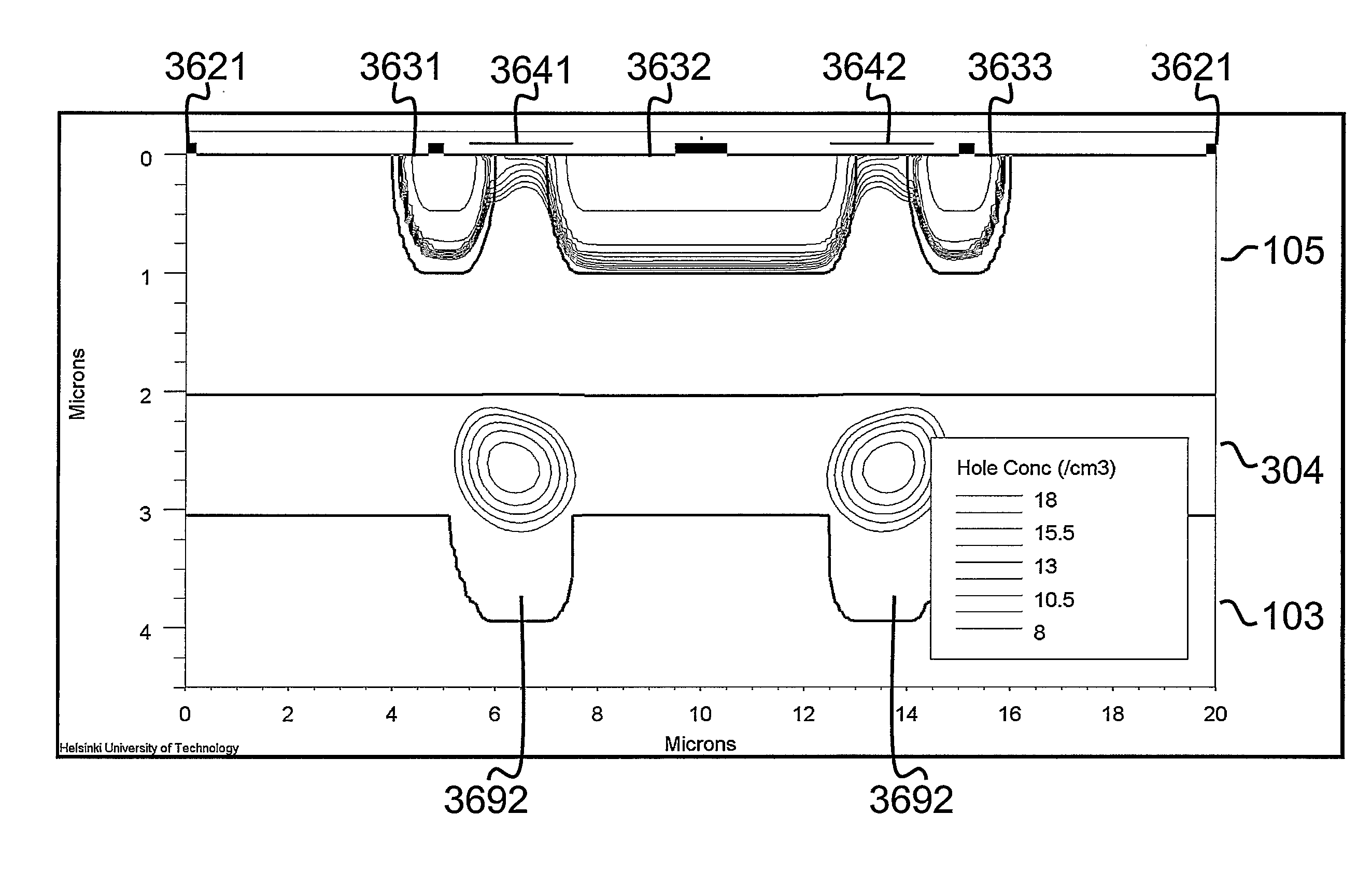
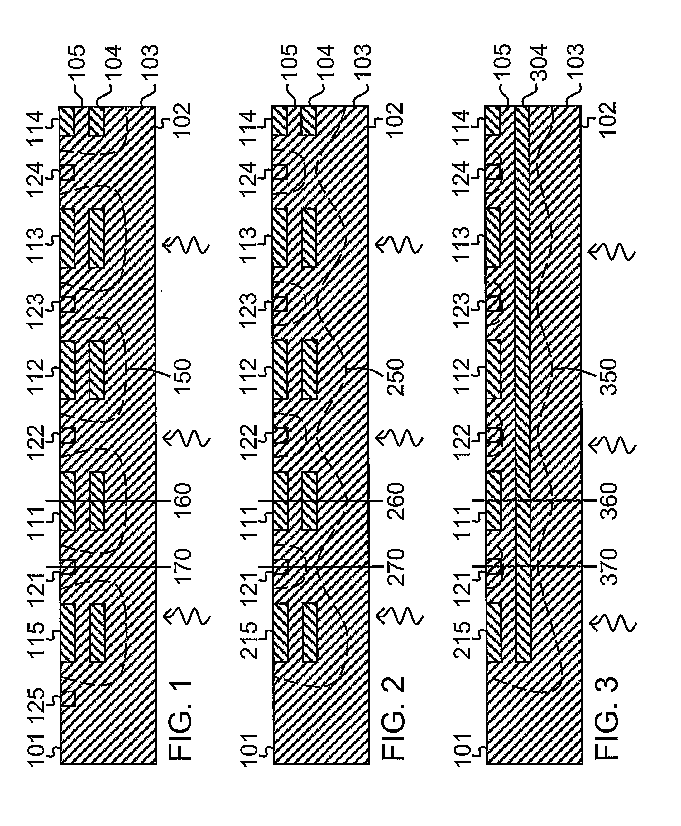
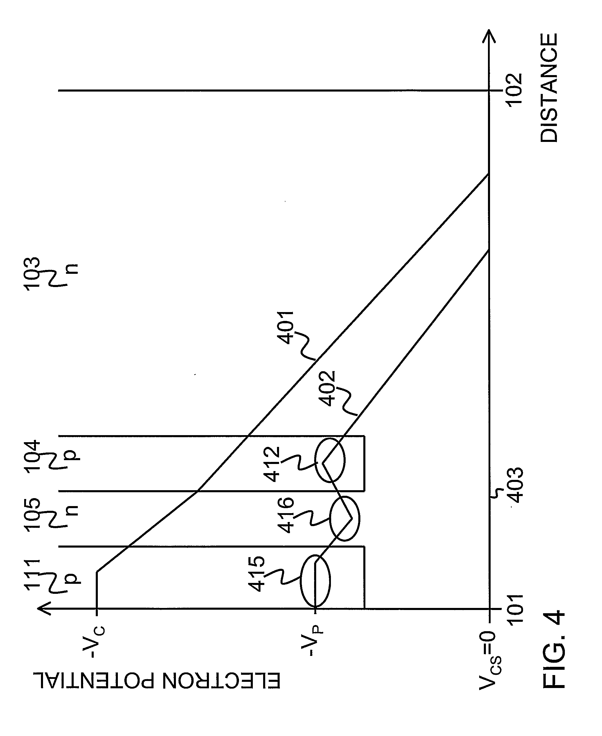
[0083]FIG. 1 is a schematic cross section of a radiation detector, which is preferably thin and back illuminated. The detector has a front surface 101 which is upwards in the drawing. The back surface 102 of the detector, through which radiation enters the detector, is downwards in the drawing. On the back surface there may be an optional antireflection or scintillator coating. The bulk layer 103 of the detector is made of semiconductor material of a first conductivity type. The first and second conductivity types or vice versa refer here to positively and negatively doped semiconductors, with an excess of positive and negative charges respectively. On the front side of the detector from the back surface towards the front surface there is first a layer 104 of the second conductivity type, which is in the following referred to as the modified internal gate (MIG) layer. In the device of FIG. 1 there are gaps in the MIG layer. In front of the MIG layer 104 there is again a layer 105 of...


PUM


Abstract

A semiconductor radiation detector comprises a bulk layer of semiconductor material, and on a first surface of the bulk layer in the following order: a modified internal gate layer of semiconductor of second conductivity type, a barrier layer of semiconductor of first conductivity type and pixel dopings of semiconductor of the second conductivity type. The pixel dopings are adapted to be coupled to at least one pixel voltage in order to create pixels corresponding to pixel dopings. The device comprises a first conductivity type first contact. Said pixel voltage is defined as a potential difference between the pixel doping and the first contact. The bulk layer is of the first conductivity type. On a second surface of the bulk layer opposite to the first surface, there is nonconductive back side layer that would transport secondary charges outside the active area of the device or function as the radiation entry window.

Description

FIELD OF THE INVENTION[0001]The invention is related to semiconductor radiation detectors and particularly to a semiconductor radiation detector having a modified internal gate.BACKGROUND OF THE INVENTION[0002]Radiation is converted to electron hole pairs in semiconductor material. In semiconductor radiation detectors the electron hole pairs are separated by an electric field. The charge type of the electron hole pair that is measured is referred to as signal charge and the opposite charge type is referred to as secondary charge.[0003]Patent applications PCT / FI2004 / 000492 and PCT / FI2005 / 000359, which are incorporated herein by reference, disclose a semiconductor radiation detector having a modified internal gate (MIG). This detector is herein after referred to as the MIG detector. The MIG detector is back-illuminated and it has a thick fully depleted substrate and a thin conductive layer on the backside of the device. This conductive backside layer has three functions: when it is pr...

Claims


Application Information

Patent Timeline
Patent Type & Authority Applications(United States)
IPC IPC(8): H01L31/00H01L21/00
CPCH01L27/14601H01L27/1464H01L27/14643H01L27/14681H01L27/14649H01L27/14679H01L27/14645H01L31/109H01L27/148
Inventor AUROLA, ARTTO
Owner AUROLA ARTTO
Why Eureka
Try Eureka