Semiconductor device and manufacturing method of the semiconductor device

a semiconductor and semiconductor technology, applied in semiconductor devices, diodes, electrical devices, etc., can solve the problems of increasing manufacturing steps, affecting the performance of semiconductor devices, and unable to obtain predetermined capacitance characteristics (data storage characteristics),

Active Publication Date: 2008-12-25
FUJITSU LTD
View PDF4 Cites 12 Cited by
  • Summary
  • Abstract
  • Description
  • Claims
  • Application Information

AI Technical Summary

Benefits of technology

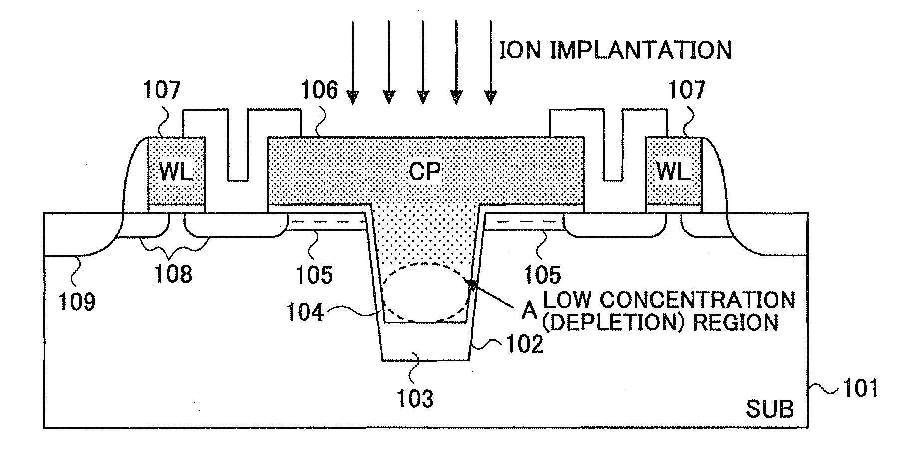
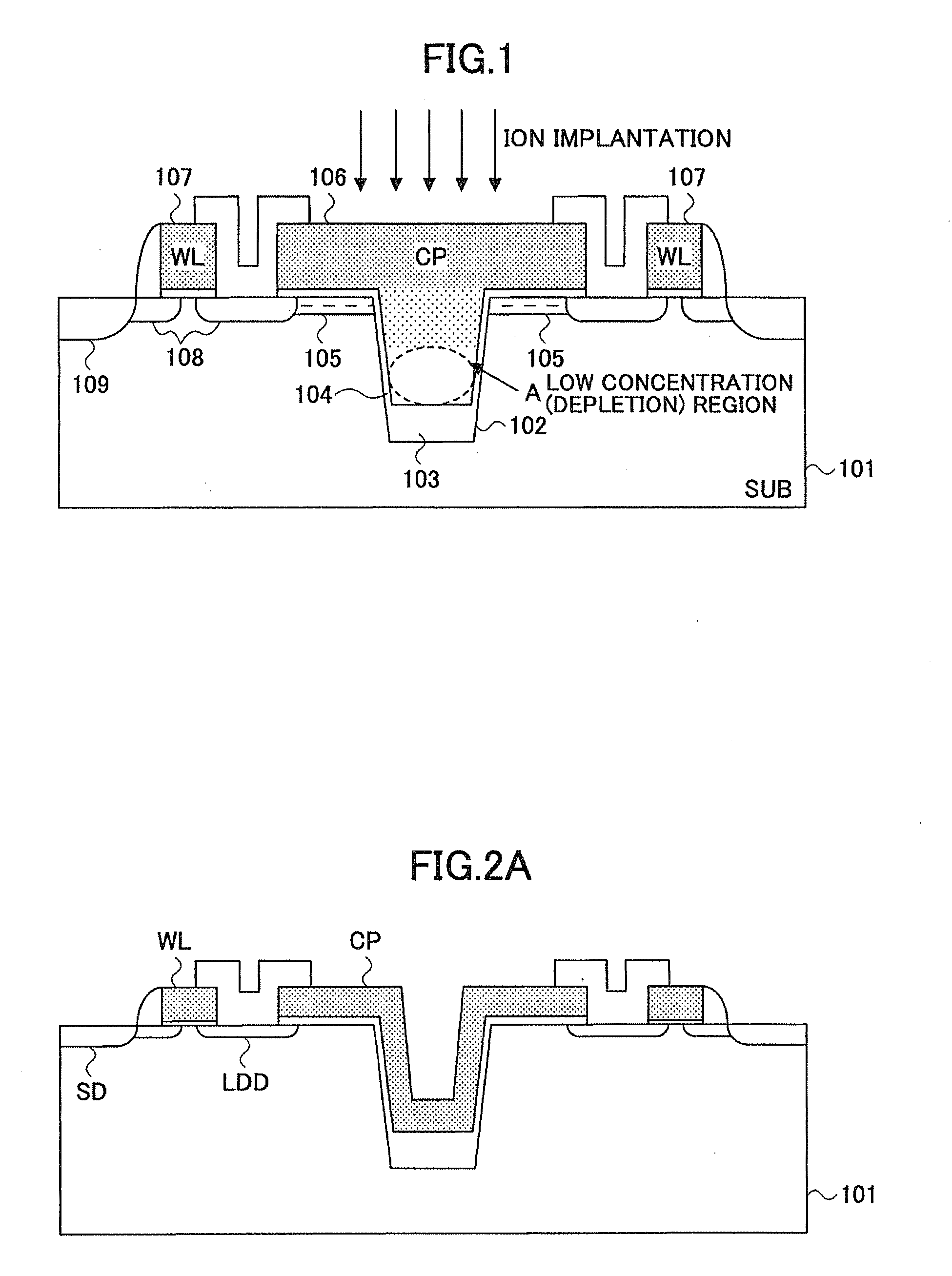
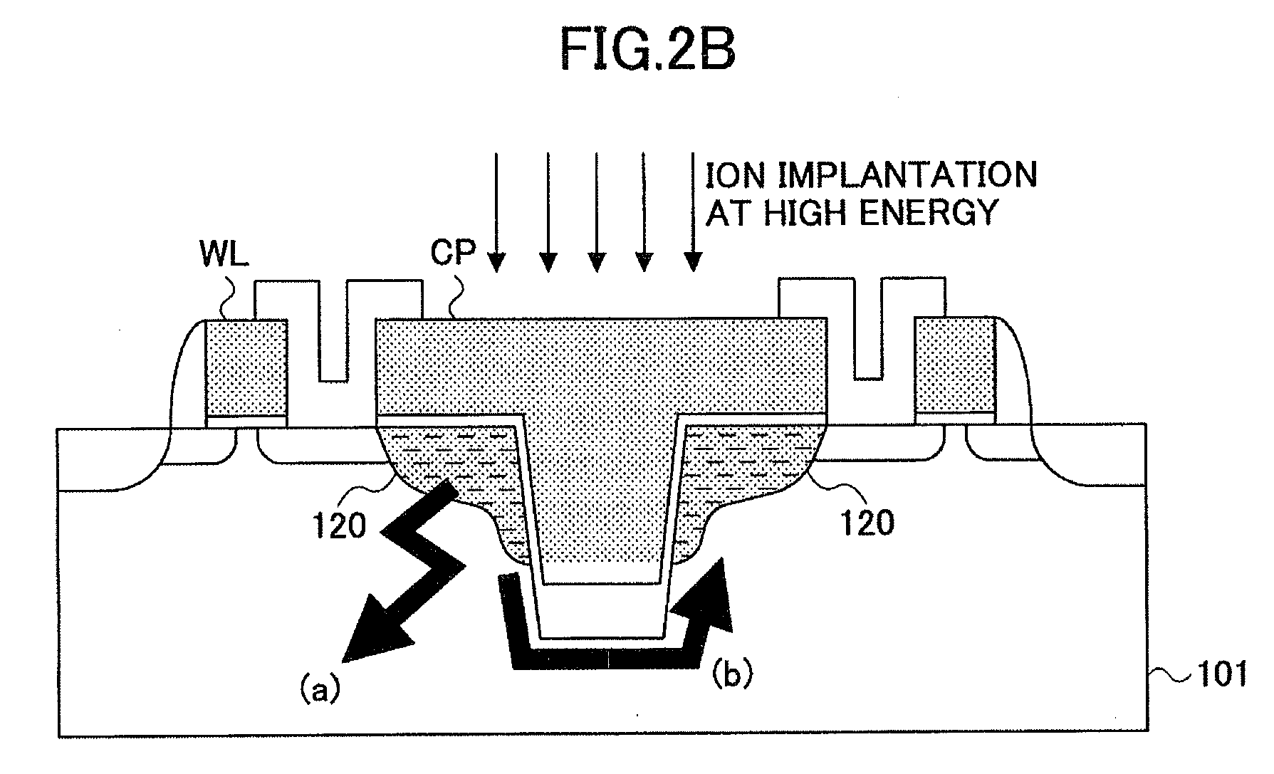
[0015]When the ion implantation is performed for a trench capacitor part and a transistor gate part by using different resist patterns, the number of fabrication steps is increased. Further, margins need to be provided for the alignment of the resist patterning. This may induce impurity penetration. As a result, an unnecessary diffusion layer 120 is formed around side walls of the trench, which causes an increase in the leakage currents (arrow (b)) between the adjacent cells and degrades the field leakage characteristics.
[0015]When the ion implantation is performed for a trench capacitor part and a transistor gate part by using different resist patterns, the number of fabrication steps is increased. Further, margins need to be provided for the alignment of the resist patterning. This may induce impurity penetration. As a result, an unnecessary diffusion layer 120 is formed around side walls of the trench, which causes an increase in the leakage currents (arrow (b)) between the adjacent cells and degrades the field leakage characteristics.
[0023]As indicated in FIG. 4(a), when a high resistance resistor element is designed by using low-resistivity resistor elements, the layout area is increased as plural low-resistivity elements need to be connected in series. Likewise, when a low resistance element is designed by using plural resistance elements with high resistivity, the units need to be connected in parallel, so that the layout area is increased as shown in FIG. 4(b). Although it is preferred that plural types of resistor elements be built on a single substrate, additional fabrication processes are necessary for fabricating such resistor elements.

Problems solved by technology

As a result, it becomes a problem that a predetermined capacitance characteristic (data storage characteristics) is not obtained.
However, each solution above causes an increase in manufacturing steps, degradation of periphery transistor characteristics, and increase in leakage currents.
This may cause degradation of periphery transistors.
However, the number of the fabrication steps increases, which increases process difficulty of the fabrication.
FIG. 2B shows a problem related to method (B) of increasing ion implantation energy.
This may cause an increase in a junction leakage current and an increase in field leakage currents between adjacent capacitors.
This may induce impurity penetration.
As a result, an unnecessary diffusion layer 120 is formed around side walls of the trench, which causes an increase in the leakage currents (arrow (b)) between the adjacent cells and degrades the field leakage characteristics.

Method used


Image

  • Semiconductor device and manufacturing method of the semiconductor device
  • Semiconductor device and manufacturing method of the semiconductor device
  • Semiconductor device and manufacturing method of the semiconductor device

Examples


Embodiment Construction

[0059]In the following, preferable embodiments are described referring to FIG. 5A through FIG. 13.

[0060]FIGS. 5A-5D are figures to describe a basic configuration. In an embodiment, for a semiconductor memory device, the side walls of STI trenches may be used for capacitors, and a cell plate electrode includes a two-layer structure. Therefore, a first poly silicon film is formed that partially fills a trench, and a second poly silicon film is formed to maintain a predetermined film thickness for forming memory cell transistors and peripheral circuit transistors; that is, there is a two-step configuration of the first poly silicon and the second poly silicon film. The first poly silicon film in the trench includes a higher impurity concentration than that of the second poly silicon film. The second poly silicon may or may not include impurities.

[0061]Specifically, as shown in FIG. 5A, a buried oxide film 13 for device isolation is provided on the bottom of a trench 14 formed on a sili...


PUM


Abstract

A semiconductor device includes a dual gate CMOS logic circuit having gate electrodes with different conducting types and a trench capacitor type memory on a same substrate includes a trench of the substrate for the trench capacitor, a dielectric film formed in the trench, a first poly silicon film formed inside of the trench, and a cell plate electrode located above the dielectric film. The cell plate electrode includes a first poly silicon film formed on the dielectric film partially filling the trench, and a second poly silicon film formed on the first poly silicon film to completely fill the trench. The second poly silicon film includes a sufficient film thickness for forming gate electrodes, wherein the impurity concentration of the first poly silicon film is higher than the impurity concentration of the second poly silicon film.

Description

CROSS-REFERENCE TO RELATED APPLICATIONS[0001]This application is a continuation application filed under 35 U.S.C. 111(a) claiming the benefit under 35 U.S.C. 120 and 365(c) of a PCT International Application No. PCT / JP2005 / 022793 filed Dec. 12, 2005, in the Japanese Patent Office, the disclosure of which is hereby incorporated by reference.BACKGROUND[0002]1. Field[0003]The embodiments discussed herein are directed to semiconductor devices and manufacturing methods of semiconductor devices, which may have trench capacitors, in which the semiconductor devices include CMOS logic circuits and one transistor-one capacitor type memory cells formed on the same substrate, and the memory cells utilize side walls of shallow trench isolation (STI) for memory capacitors and a manufacturing method of the semiconductor device.[0004]2. Description of the Related Art[0005]For semiconductor memories that include memory cells to store data in capacitors, trench capacitor type semiconductor memories a...

Claims


Application Information

Patent Timeline
Patent Type & Authority Applications(United States)
IPC IPC(8): H01L29/00H01L21/20
CPCH01L21/84H01L27/0629H01L27/10829H01L27/1087H01L27/10894H01L29/66181H01L29/945H01L27/1052H10B99/00H10B12/37H10B12/0387H10B12/09
Inventor ASANO, MASAYOSHISUZUKI, YOSHIYUKIITO, TETSUYAWADA, HAJIME
Owner FUJITSU LTD
Why Eureka
Try Eureka