Low Power All Digital PLL Architecture

a phaselocked loop, low-power technology, applied in the field of circuits, can solve the problems of large current leakage, large current leakage, and the general coarse phase/frequency resolution of prior-art architectures, and achieve the effect of reducing circuit complexity, high speed of new transistors, and reducing nois

Active Publication Date: 2008-12-25
TEXAS INSTR INC
View PDF7 Cites 35 Cited by
  • Summary
  • Abstract
  • Description
  • Claims
  • Application Information

AI Technical Summary

Benefits of technology

[0008]The present invention provides a circuit and architecture for an all-digital PLL that makes use of modern IC semiconductor process technology advantages such as the high speed of the new transistors (e.g. deep-submicron MOSFET) as well as fine device matching, and that reduce the complexity of circuits such as the TDC in the PLL. The reduction in circuitry reduces the noise and improves linearity. The new PLL is compact, low-power and still delivers high phase noise performance. Low power is achieved by creating an architecture with low complexity circuits and minimizing the percentage of high speed digital circuit, and by turning off some circuits under various conditions.

Problems solved by technology

However, the digital solution has also presented new problems in addition to the generally coarser phase / frequency resolution of prior-art architectures.
The new technologies have transistors with large current leakage and power savings became a big problem.
Performance issues such as better linearity is desired but often difficult to achieve.
Finally, lower complexity and lower die area are highly desirable, but again difficult to achieve.

Method used


Image

  • Low Power All Digital PLL Architecture
  • Low Power All Digital PLL Architecture
  • Low Power All Digital PLL Architecture

Examples


Embodiment Construction

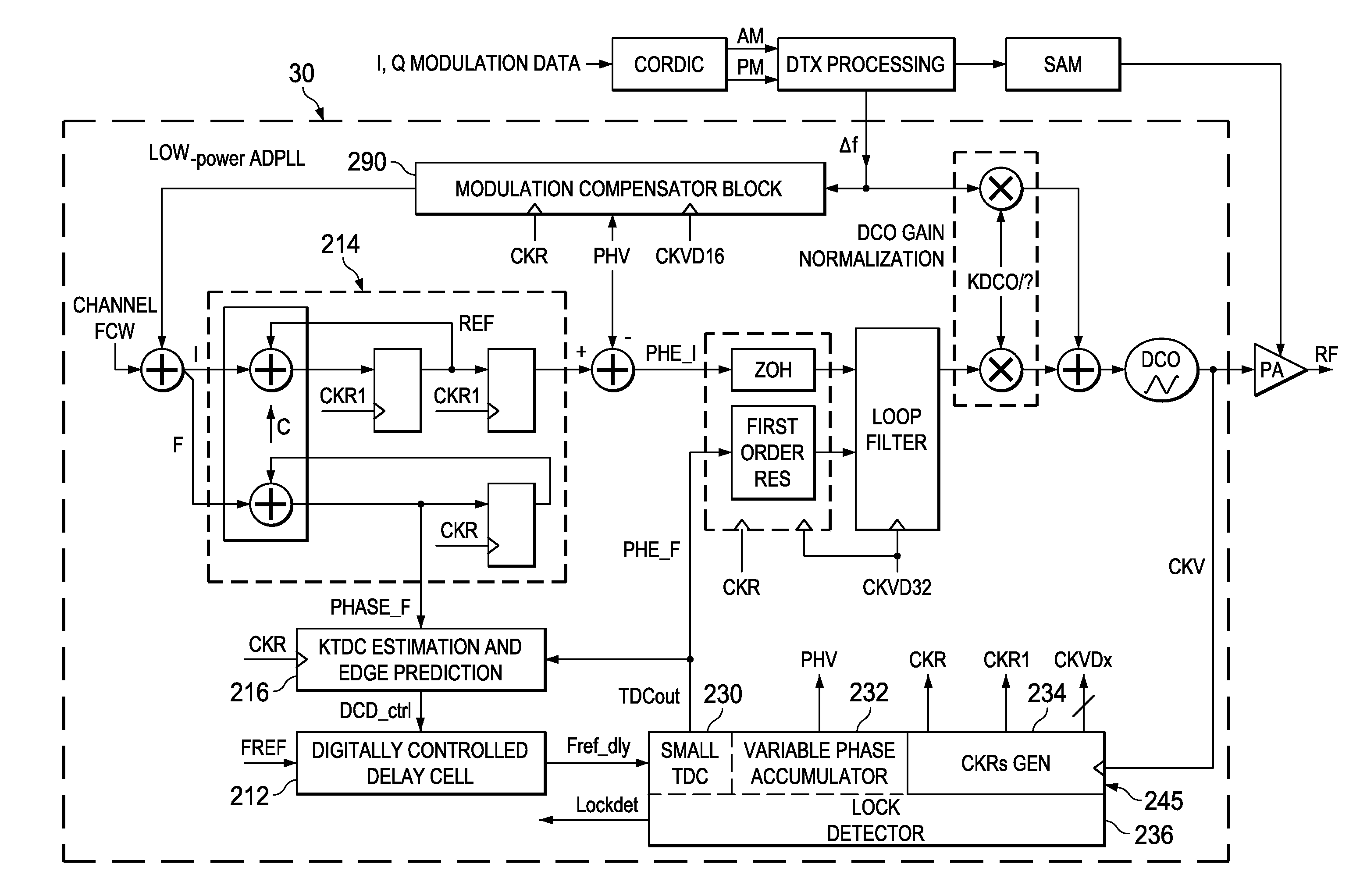
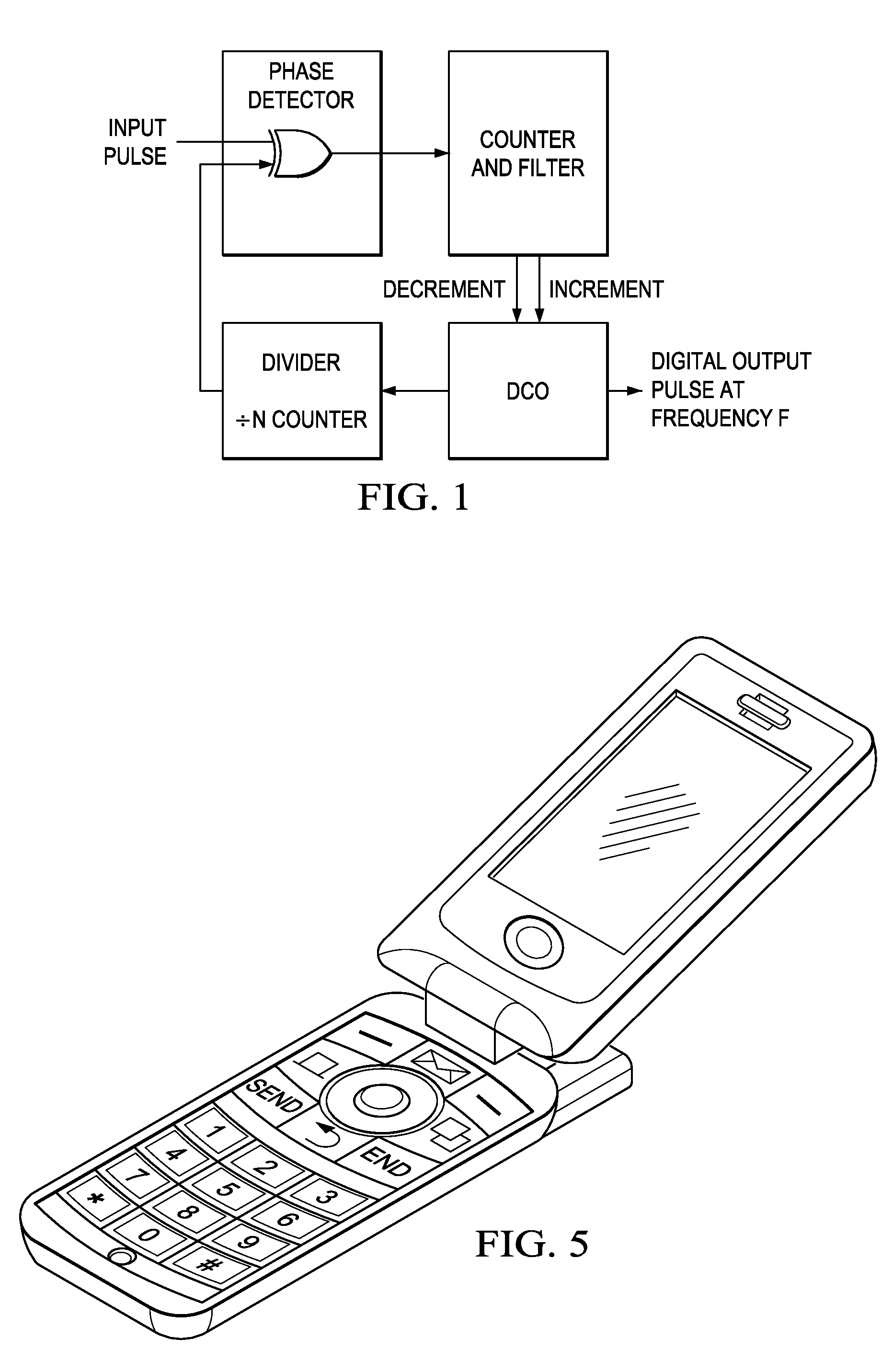
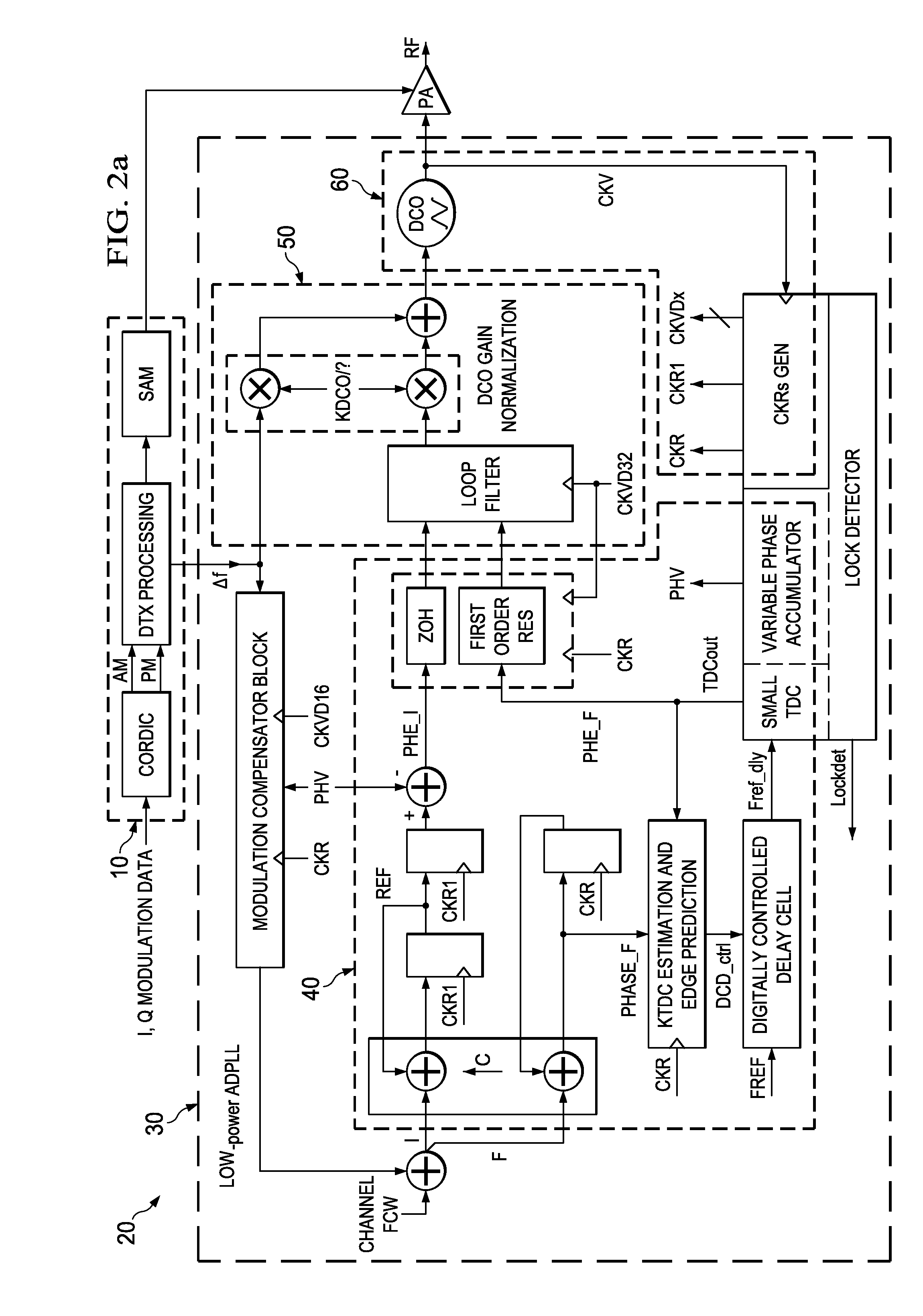
[0018]FIG. 1 is discussed above in the Background of the Invention section of this document and the reader is assumed familiar with the principles of that discussion. To provide an example setting for an all-digital PLL (ADPLL) in a wireless application, FIG. 2 (a and b) shows three main circuit blocks, a baseband signal transmitter block 10, an RF power amplifier with a digital gain control 20 and an ADPLL 30 with frequency modulation capability. The ADPLL contains many sub-circuits including a digitally-controlled oscillator (DCO). The three main circuit blocks together may provide a digital RF radio output signal for a wireless system, such as for a mobile handset (FIG. 5). The transmitter block 10 provides amplitude and phase modulated conversions (CORDIC) of the typical I and Q signals of a baseband codec to a digital transmitter processor (DTX), then further to a sigma-delta amplitude modulator block (SAM) to control the amplitude of the power amplifier 20. The DTX sends phase...


PUM


Abstract

A new all digital PLL (ADPLL) circuit and architecture and the corresponding method of implementation are provided. The ADPLL processes an integer and a fractional part of the phase signal separately, and achieves power reduction by disabling circuitry along the integer processing path of the circuit when the ADPLL loop is in a locked state. The integer processing path is automatically enabled when the loop is not in lock. Additional power savings is achieved by running the ADPLL on the lower-frequency master system clock, which also has the effect of reducing spur levels on the signals.

Description

CROSS-REFERENCES TO RELATED APPLICATIONS[0001]This application claims the benefit of the filing date of copending provisional application U.S. Ser. No. 60 / 945,821, filed Jun. 22, 2007, entitled “Low Power ADPLL Architecture” to Zhuang et al.STATEMENT REGARDING FEDERALLY SPONSORED RESEARCH OR DEVELOPMENT[0002]Not Applicable.FIELD OF THE INVENTION[0003]The present embodiments relate to circuits such as on a chip (IC) or to circuits with discrete components such as on a printed circuit board (PCB) and are more particularly directed to an all-digital phase-locked loop (ADPLL) circuit and architecture.BACKGROUND OF THE INVENTION[0004]Electronic systems often include PLL's as a basic building block to stabilize a particular communications channel (keeping it set to a particular frequency), to generate a signal, modulate or demodulate a signal, reconstitute a signal with less noise, or multiply or divide a frequency. PLLs are frequently used in wireless communication, particularly where si...

Claims


Application Information

Patent Timeline
Patent Type & Authority Applications(United States)
IPC IPC(8): H03L7/00
CPCH03C5/00H03L7/0814H03L2207/50
Inventor ZHUANG, JINGCHENGSTASZEWSKI, ROBERT BOGDAN
Owner TEXAS INSTR INC
Why Eureka
Try Eureka