Method of manufacturing silicon carbide semiconductor substrate

a technology of silicon carbide and semiconductor substrate, which is applied in the direction of crystal growth process, polycrystalline material growth, chemically reactive gas growth process, etc., can solve the problems of frequent unsatisfactory characteristics of semiconductor devices, difficult to perform, and inability to use si power devices under such conditions, so as to reduce the density of basal plane dislocations (bpds) and flatten the irregularities

Inactive Publication Date: 2008-12-25
FUJI ELECTRIC CO LTD
View PDF2 Cites 27 Cited by
  • Summary
  • Abstract
  • Description
  • Claims
  • Application Information

AI Technical Summary

Benefits of technology

[0019]By means of this invention, a method of manufacturing silicon carbide semiconductor substrates can be provided which reduces the density of basal plane dislocatio

Problems solved by technology

However, power devices are also used at high temperatures or in the presence of radiation, and in some cases Si power devices cannot be used under such conditions.
However, when using an SiC semiconductor substrate to manufacture a semiconductor device, ion implantation and impurity doping by thermal diffusion, which are normally indispensable process technologies for Si semiconductor devices, are difficult to perform; hence simultaneously with impurity doping control, epitaxial growth layers are formed in the required number of layers on the low-resistance SiC substrate (SUB), to manufacture an SiC semiconductor device having the desired semiconductor functions.
However, such SiC semiconductor devices have the problem of frequent unsatisfactory characteristics, arising from crystal defects.
However, as is also described in the above references, numerous lattice defects and dislocations exist

Method used


Image

  • Method of manufacturing silicon carbide semiconductor substrate
  • Method of manufacturing silicon carbide semiconductor substrate

Examples


embodiment 1

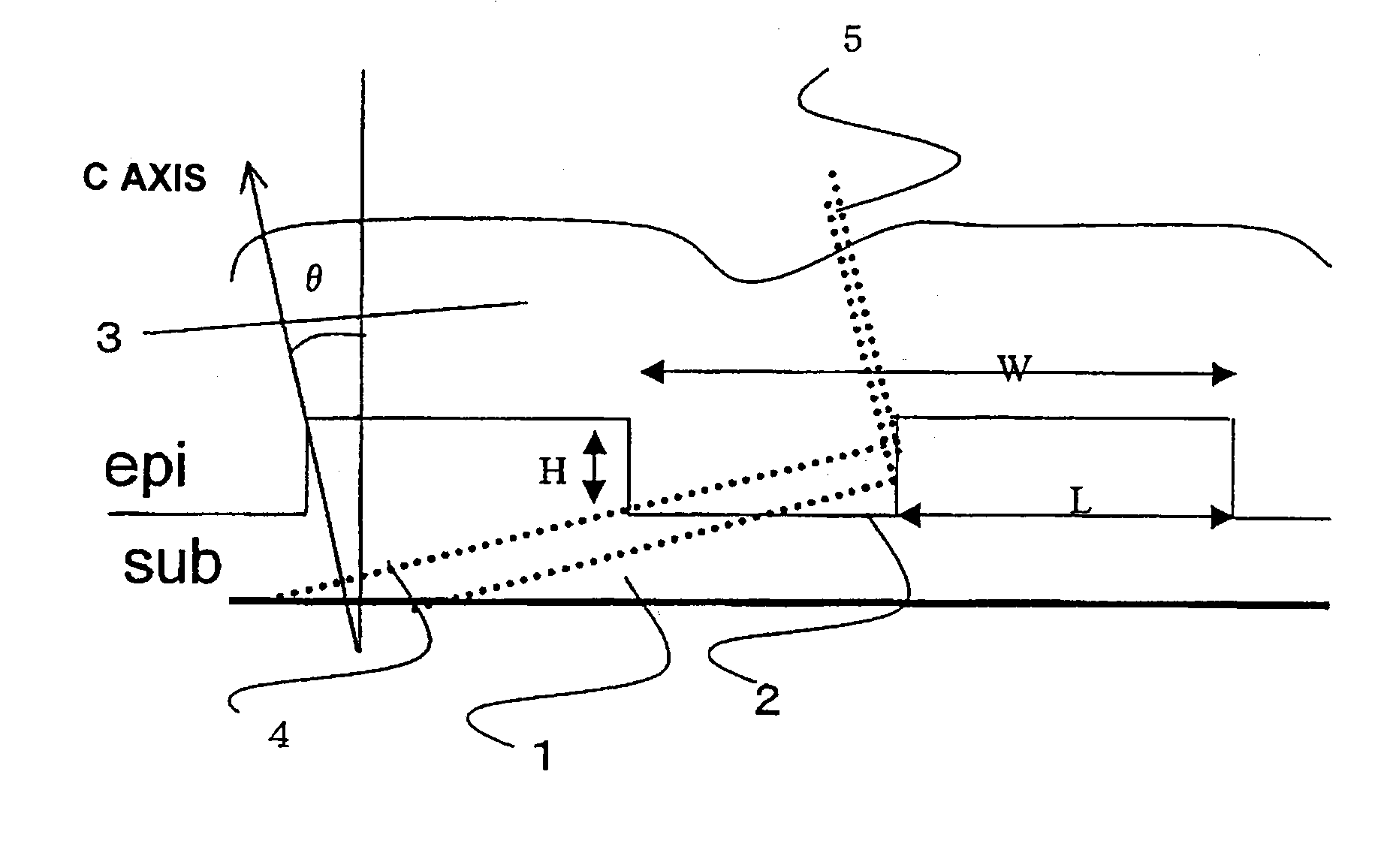
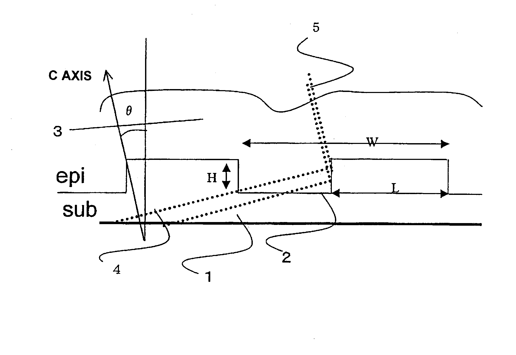
[0023]As the substrate prior to epitaxial growth (hereafter abbreviated to “SiC substrate” or “SUB”), an N (nitrogen)-doped n-type SiC substrate (1018 cm−3) 4-H SiC single crystal, subjected to mirror polishing and CMP treatment, was used; a face polished so as to be inclined by 80 from the (0001)Si plane in the direction was used.

[0024]Trenches 2 were formed on the surface of the SiC substrate by ICP (Inductive Coupled Plasma) etching in a straight line, in a direction perpendicular to the direction of SiC substrate 1, using an oxide film as a mask. The drawing FIGURE shows a cross-sectional view of SiC substrate 1 with these trenches 2 formed. At this time, the trench depth H is set to 0.5 μm, the protruding portion width is set to 0.5 μm, and the trench interval (repetition pitch) W is set to 1.0 μm, such that basal plane dislocations (BPDs) 4 which grow always reach a trench side wall during SiC epitaxial growth. When basal plane dislocation (BPD) 4 reaches a trench side wall,...


PUM


Abstract

A method of manufacturing a silicon carbide semiconductor substrate is disclosed in which the density of basal plane dislocations (BPDs) in particular is reduced in an SiC crystal substrate. Irregularities in the surface of the substrate due to this reduction also can be flattened. A method of manufacturing a silicon carbide semiconductor substrate is disclosed in which, prior to forming an epitaxial growth layer on a silicon carbide substrate with an off-axis angle of 1° to 8°, parallel line-shape irregularities, which have an irregularity cross-sectional aspect ratio equal to or greater than the tangent of the off-axis angle of the silicon carbide substrate, are formed in the substrate surface. The irregularites have a height between 0.25 μm and 5 μm.

Description

CROSS REFERENCE TO RELATED APPLICATIONS[0001]This application claims priority from Japanese application Serial No. 2007-159643, filed on Jun. 18, 2007. The disclosure of the priority application in its entirety, including the drawing, claims, and the specification thereof, is incorporated herein by reference.BACKGROUND OF THE INVENTION[0002]A. Field of the Invention[0003]This invention relates to a method of manufacturing a silicon carbide semiconductor substrate.[0004]B. Description of the Related Art[0005]Various measures are being taken to enhance the performance of semiconductor devices for power applications (hereafter “power devices”) using silicon semiconductor substrates (hereafter abbreviated “Si”), for the purpose of controlling large amounts of power. However, power devices are also used at high temperatures or in the presence of radiation, and in some cases Si power devices cannot be used under such conditions.[0006]Also, in response to requests for still higher performa...

Claims


Application Information

Patent Timeline
IPC IPC(8): H01L21/205
CPCC30B23/02C30B25/02C30B25/18C30B29/36H01L21/02378H01L21/02529H01L21/0262H01L21/02634H01L21/02658
Inventor YONEZAWA, YOSHIYUKITAWARA, TAKESHI
Owner FUJI ELECTRIC CO LTD
Why Eureka
Try Eureka