
Probing device

a probe card and probe technology, applied in the direction of solid-state devices, semiconductor/solid-state device testing/measurement, instruments, etc., can solve the problems of affecting the test, requiring much cost and labor time, and complicated fabrication of this design of the probe card, so as to achieve high quality transmission characteristics, high structural strength, and high efficiency

Inactive Publication Date: 2009-01-08
MICROELECTRONICS TECH INC
View PDF2 Cites 12 Cited by
  • Summary
  • Abstract
  • Description
  • Claims
  • Application Information

AI Technical Summary

Benefits of technology

[0008]It is another object of the present invention to provide a probing device, which has high efficiency and low cost characteristics.
[0009]It is still another object of the present invention to provide a probing device, which effectively isolates the internal signal lines from external moisture.
[0010]To achieve these and other objects of the present invention, a probing device is provided for transmitting test signals from a tester to an IC wafer for testing electric characteristics of the IC wafer. The probing device comprises a rack that has an outer support member extending around the periphery and supporting a circuit layer and a center support member disposed at the center and supporting a probe assembly. When the tester touching down the circuit layer of the probing device from the top side, the outer support member of the rack bears this touchdown stress. When the probes of the probe holder touching down the electronic components of an IC wafer under test, the center support member of the rack bears the reaction force from the IC wafer. Therefore, the high structural strength of the rack is practical for supporting any equivalent circuit layer and probe assembly structure capable of transmitting the test signals from the tester to the IC wafer to be tested. Further, because the circuit layer has an electrically insulated material structure of which the layer thickness is thinner than a typical conventional multi-layer printed circuit board, the traveling path of each test signal that goes through the circuit layer is short, effectively eliminating the problem of leakage current effect between each two adjacent transmission signals as seen in the prior art designs and also eliminating the drawback of complicated manufacturing process of the multi-layer printed circuit board type prior art design.

Problems solved by technology

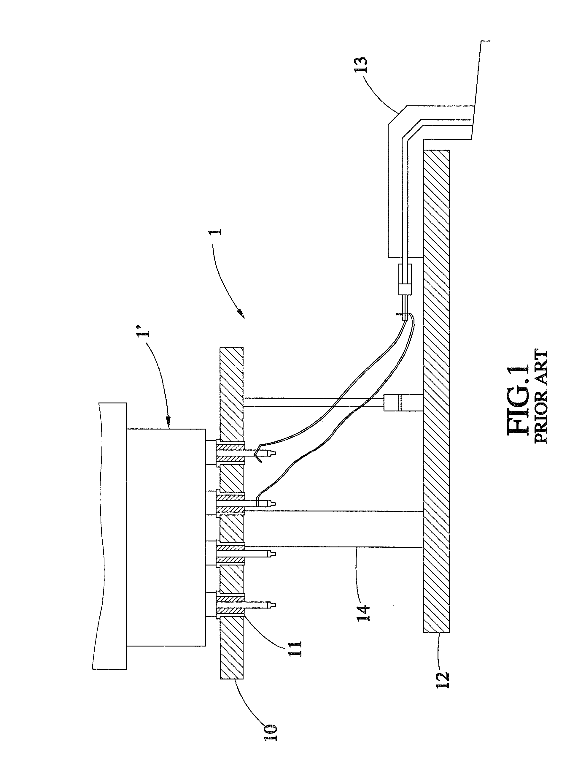
During the whole wafer level testing process, the circuit transmission design of the circuit board of the probe card greatly affects the test result.
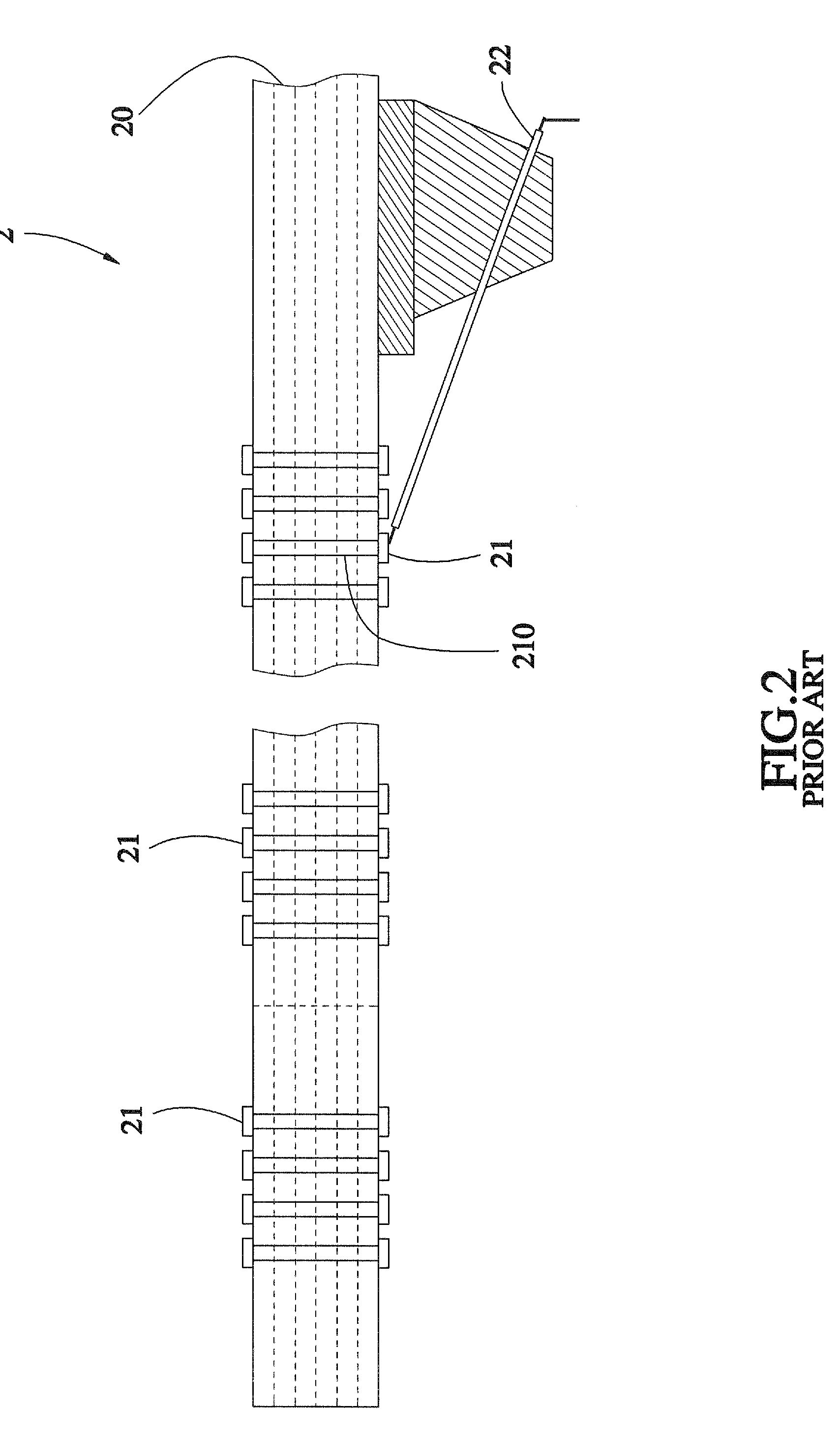
However, because the multi-layer printed circuit board 20 is a lamination of multiple layers of glass fiber or ceramic material and because each layer has metal wires arranged thereon to form the circuit lines 21, the fabrication of this design of probe card is complicated, requiring much cost and labor time.
Further, the via holes 210 of the multi-layer printed circuit board 20 through which the circuit lines 21 extend tend to cause interface reflection during transmission of test signals, resulting in energy loss.
These drawbacks greatly affect high frequency transmission characteristics.
Therefore, this design of probe card does not meet the requirements for high speed test of integrated electronic components.

Method used


Image

  • Probing device
  • Probing device
  • Probing device

Examples


first embodiment

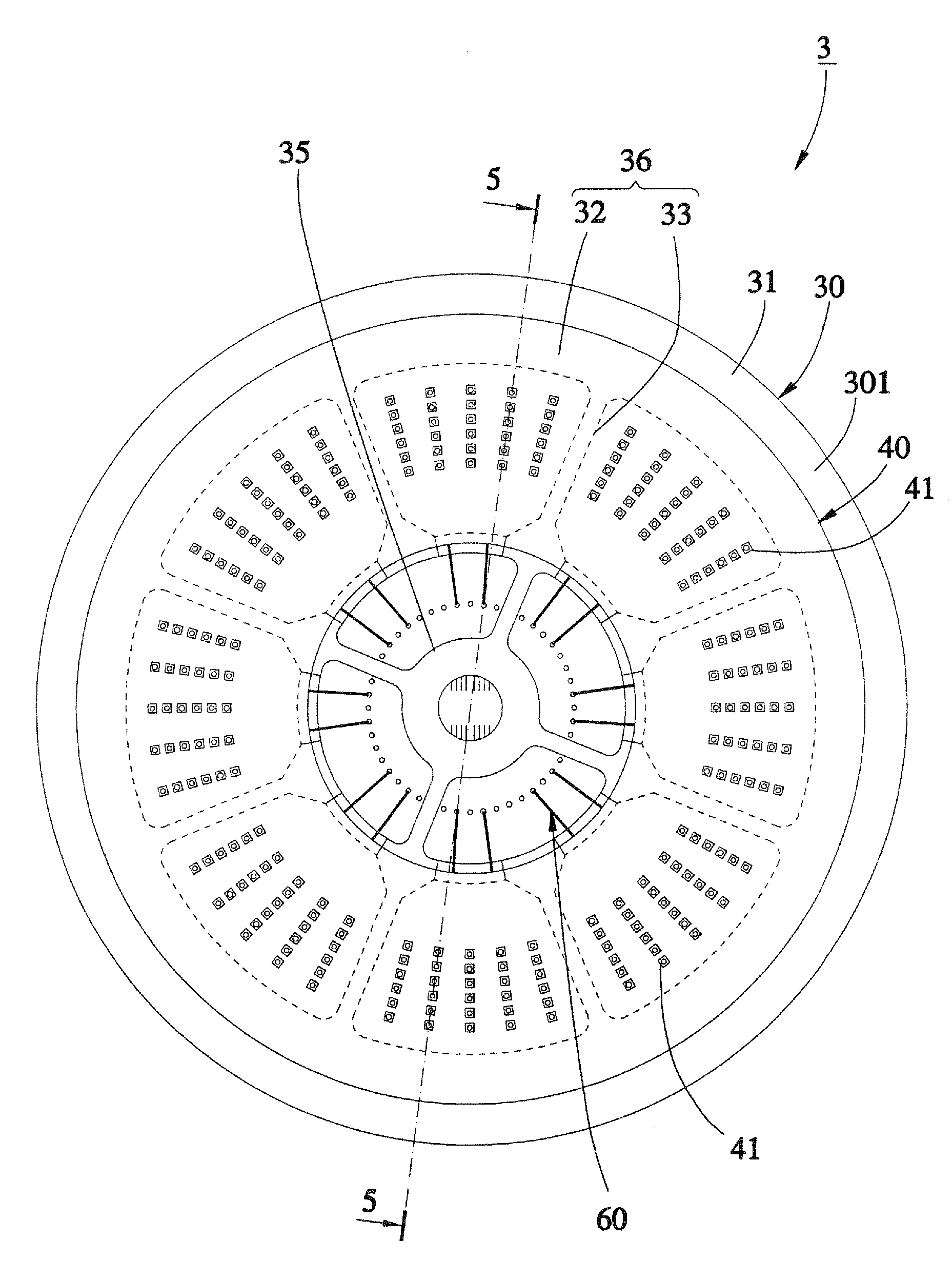
[0034]Referring to FIGS. 3˜5, a probing device 3 in accordance with the present invention is shown for transmitting test signals from a tester to an IC wafer for measuring electric characteristics of the IC wafer. The probing device 3 comprises a rack 30, a circuit layer 40, a cantilever probe assembly 50, and multiple signal lines 60.

[0035]Referring to FIG. 6 and FIG. 5 again, the rack 30 is a rigid annular member having a certain strength and a dimension approximately equal to a semiconductor IC wafer. The rack 30 can be integrally formed of metal (for example, stainless steel), having a thickness corresponding to a regular typical multi-layer printed circuit board to bear stress during test operation, without causing deformation of the planarity of the rigid body. The rack 30 has a top surface 301, and a bottom surface 302 opposite to the top surface 301. The rack 30 further has, arranged in proper order from the periphery toward the center, a first ring portion 31, a second ring...

sixth embodiment

[0064]Therefore, the probing device 5′ of this sixth embodiment utilizes the rigid structure of the rack 80′ to support the circuit layer 45′ at the top side and the vertical probe assembly 90′ at the bottom side, effectively bearing the stress received by the circuit layer 45′ and the vertical probe pin set 90′. Further, because the vertical probe assembly 90′ are directly connected to the signal lines 65′, the signal lines 65′ directly transfer test signals from the tester to the probes 94′, and therefore no any intermediate adapter circuit means between the signal lines 65′ and the probes 94′ is necessary.


PUM


Abstract

A probing device includes a rack that has an outer support member supporting a circuit layer and a center support member supporting a probe assembly. When the tester touching down the circuit layer of the probing device from the top side, the outer support member of the rack bears this touchdown stress. When the probes of the probe holder touching down the electronic components of an IC wafer under test, the center support member of the rack bears the reaction force from the IC wafer.

Description

BACKGROUND OF THE INVENTION[0001]1. Field of the Invention[0002]The present invention relates to test device and more particularly, to a probing device for testing IC wafers.[0003]2. Description of the Related Art[0004]When testing an IC wafer, a probe card is used for transmitting test signals from a tester to the IC wafer. A typical conventional probe card comprises a circuit board for touchdown by the test head of a tester and receiving test signals from the tester, and a plurality of probes arranged in a high density manner at the center area of the bottom side of the circuit board for transmitting test signals from the circuit board to the IC wafer under test. After the probes touched down the electronic components of the IC wafer under test, test signals are transmitted from the tester to the electronic components of the IC wafer through the probe card, and measured signals are transmitted backwards from the electronic components of the IC wafer through the probe card to the t...

Claims


Application Information

Patent Timeline
Patent Type & Authority Applications(United States)
IPC IPC(8): G01R1/073
CPCG01R1/06772G01R31/2889H01L2924/0002H01L2924/00H01L22/00G01R1/067
Inventor KU, WEI-CHENGHO, CHIH-HAOLIN, HO-HUIFENG, TE-CHENLAI, JUN-LIANGHO, JIA-CHICHIEN, CHIH-CHUNGHUANG, CHIEN-HUEICHANG, AI-CHUANSUN, HORNG-CHUAN
Owner MICROELECTRONICS TECH INC
Learn More