

Method of Manufacturing Vanadium Oxide Thin Film
a vanadium oxide and thin film technology, applied in the field of manufacturing vanadium oxide thin films, can solve the problems of increasing the cost of the method, and achieve the effect of uniform thickness and stable composition
- Summary
- Abstract
- Description
- Claims
- Application Information
AI Technical Summary
Benefits of technology
Problems solved by technology
Method used
Image

Examples
first embodiment
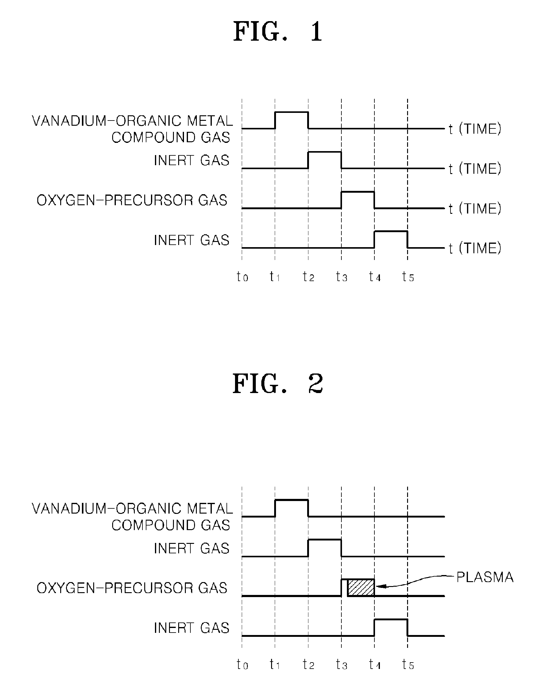
[0033]FIG. 1 is a timing diagram for explaining an ALD method of manufacturing a vanadium oxide thin film according to a first embodiment of the present invention.
[0034]Referring to FIG. 1, a substrate is loaded in a chamber (t0-t1). After that, a vanadium-organometallic compound, which is a precursor of vanadium, is injected into the chamber so that an adsorption layer of vanadium precursor molecules are formed on the surface of the substrate by surface saturation adsorption (t1-t2). Here, the surface saturation adsorption means that adsorption does not occur any more after the vanadium precursor molecules are all adsorbed in a monolayer on the surface of the substrate even when excess amount of precursor molecules is injected. An inert gas, e.g., a nitrogen or argon (Ar) gas is injected into the chamber in order to purge out a vanadium-organometallic compound gas that remains in the chamber and is not adsorbed (t2-t3). An oxygen precursor (oxidant) is injected into the chamber to ...
second embodiment
[0038]FIG. 2 is a timing diagram for explaining a PEALD method according to a second embodiment of the present invention. The second embodiment is the same as the first embodiment except that the oxygen plasma, which is an oxygen precursor, is utilized.
[0039]Referring to FIG. 2, the oxygen plasma is generated during the injection of oxygen step (t3-t4). The oxygen plasma may be maintained for the same time as or shorter than the injection time, t3-t4, of the oxygen precursor. In detail, the plasma may be generated simultaneously with the injection of the oxygen into the chamber, or may be generated when a predetermined period of time elapses during the injection of oxygen. The plasma may be generated directly within a reaction chamber, or may be formed through a remote manner in which reactive particles are generated in an adjacent plasma chamber and injected into a reaction chamber.
[0040]In the PEALD method according to the second embodiment of the present invention, deposition is ...
experimental examples
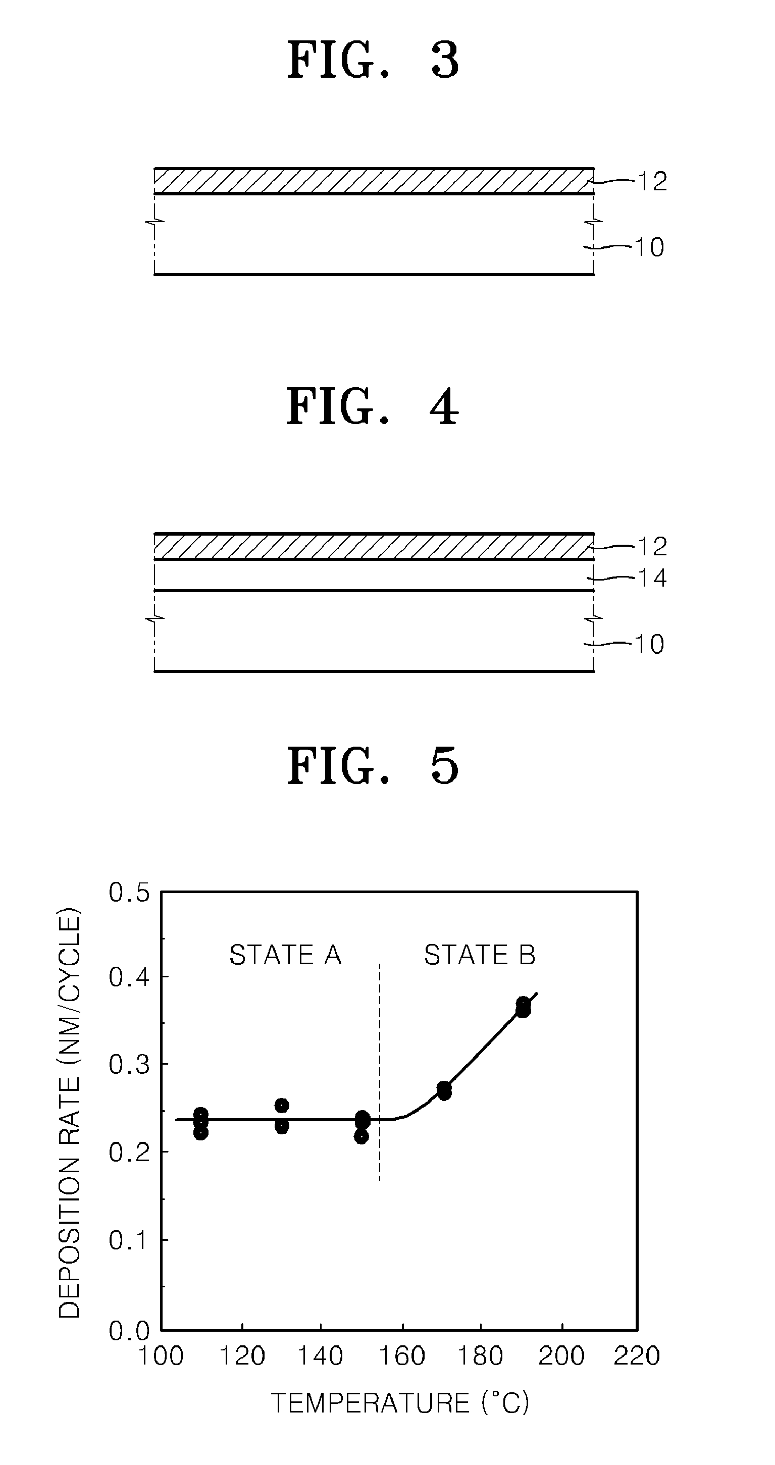
[0042]A device containing the vanadium oxide thin film (referred to as a vanadium oxide film 12 hereinafter) described in the second embodiment is manufactured as explained with reference to FIGS. 3 and 4. FIG. 4 illustrates a buffer layer 14 that is further formed in the device illustrated in FIG. 3, if necessary.
[0043]To manufacture the vanadium oxide film 12, a silicon substrate 10 with a diameter of 2-12 inch is loaded to the reaction chamber first. After that, (1) tetraethylmethylamino vanadium (V{N(C2H5CH3)}4) (TEMAV) vapor is injected into a chamber to adsorb to form a saturated adsorption layer on the Si surface 10, and (2) an inert gas is injected into the chamber to purge out a gas remaining therein. Next, (3) an oxygen gas is injected into the chamber and oxygen plasma is generated, then the energetic particles of oxygen plasma react with the adsorbed vanadium precursors to form a monolayered vanadium oxide film 12. After that, (4) an inert gas is injected into the chambe...
PUM
| Property | Measurement | Unit |
|---|---|---|
| diameter | aaaaa | aaaaa |
| vapor pressure | aaaaa | aaaaa |
| temperature | aaaaa | aaaaa |
Abstract
Description
Claims
Application Information