

Silicon epitaxial wafer and production method for same
a technology of epitaxial wafers and production methods, applied in the direction of sustainable manufacturing/processing, instruments, radiological control devices, etc., can solve the problems of reducing the yield of imaging devices, image cannot be captured at the position of white defects, and white defects, etc., to achieve optimum applicability to production, improve yield, and the effect of sufficient ig
Inactive Publication Date: 2009-01-15
SUMCO CORP
View PDF10 Cites 15 Cited by
- Summary
- Abstract
- Description
- Claims
- Application Information
AI Technical Summary
Benefits of technology
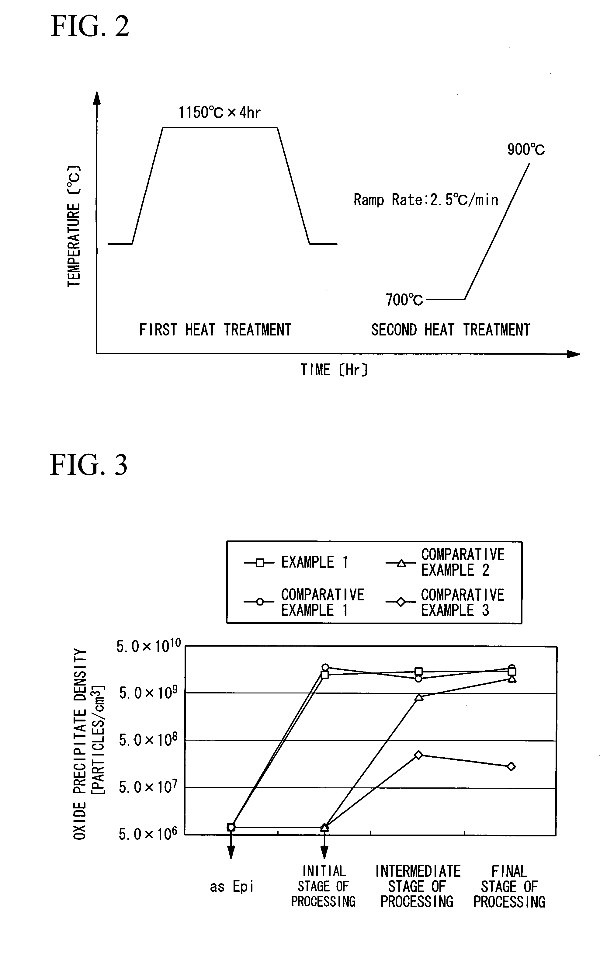
[0018]An epitaxial wafer of the present invention generates oxide precipitates of not less than 5×10⁹ particles / cm3 in the early stage of the production process of an imaging device and therefore provides a sufficient IG effect. In addition, an EG effect is provided by the polycrystalline silicon layer. Therefore, the silicon epitaxial wafer has an optimum applicability to the production of an imaging device which is sensitive to heavy metal contamination, and contributes to improvement of the yield.
[0019]By a method for producing an epitaxial wafer according to the invention, it is possible to produce an epitaxial wafer at lower cost than that of the DZ-IG wafer, which requires high production cost and has a high possibility of heavy metal contamination occurring in its production process. In addition, since there is no need for a high-temperature heat treatment, contamination with heavy metals does not occur in the device production process and a strong gettering effect can be expected from the early stage of the production process of an imaging device.
Problems solved by technology
Where a white defect occurs in an imaging element, an image cannot be captured at the position of the white defect.
Therefore, a white defect causes a problem of reducing the yield of the imaging device.
It is known that the white defect is caused by contamination of heavy metals in a silicon wafer.
Since the DG-IG heat treatment generally requires a treatment time of 10 hours or more, the production cost of the DG-IG wafer is expensive.
In addition, the DZ heat treatment performed at a high temperature has allowed a possibility of contamination of the wafer with heavy metals during the heat treatment.
Therefore, the DZ-IG wafer produced using the DZ-IG wafer also had a problem of high production cost and the occurrence of heavy metal contamination during the heat treatment.
Method used
View moreImage
Smart ImageViewing Examples

Examples
example 1
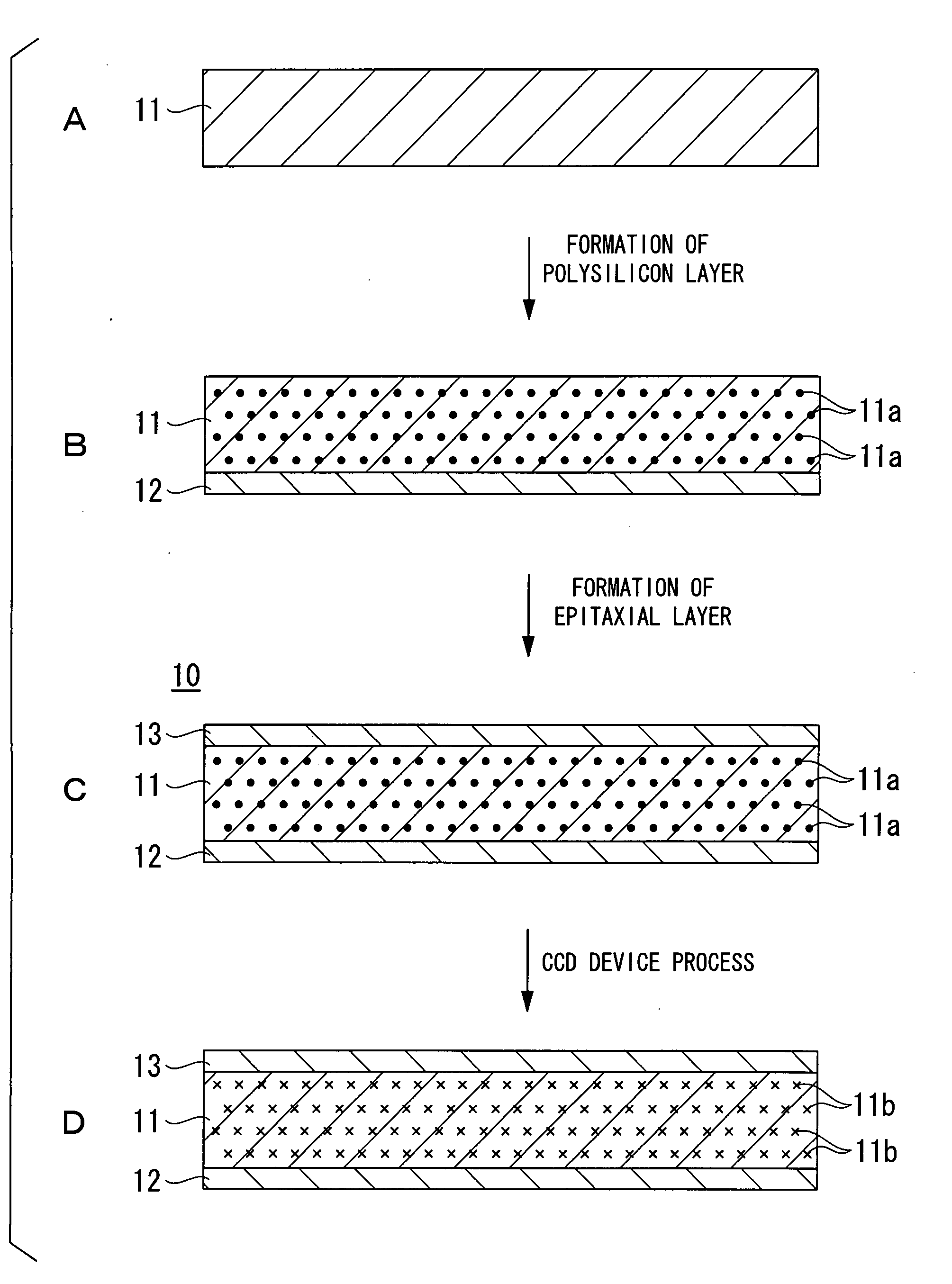
[0040]Firstly, a silicon ingot doped with P at a concentration of 4.4×10¹⁴ atoms / cm3 and carbon at a concentration of 1×10¹⁶ atoms / cm3 (ASTM F123-1981), having an oxygen concentration of 15×1017 atoms / cm3 (ASTM F121-1979), and having a resistivity of 10 Ω·cm was grown by the CZ method. Then, n-type silicon wafers having a diameter of 8 inches were sliced from the ingot. Next, a polycrystalline silicon layer of 1 μm in thickness was formed on a backside of the silicon single crystal wafer. Next, on the front surface of the silicon single crystal wafer, an epitaxial layer of n-type silicon single crystal having a resistivity of 10 Ω·cm was epitaxially grown so as to have a thickness of 10 μm. Thus, an epitaxial wafer was obtained.
Login to View More PUM
| Property | Measurement | Unit |
|---|---|---|
| thickness | aaaaa | aaaaa |
| thickness | aaaaa | aaaaa |
| temperature | aaaaa | aaaaa |
Abstract
A silicon epitaxial wafer of the invention comprises a silicon single crystal wafer sliced from a CZ silicon ingot doped with carbon in a concentration range of not less than 5×10¹⁵ atoms / cm3 and not more than 5×10¹⁷ atoms / cm3 and an epitaxial layer consisting of a silicon single crystal epitaxially grown on a front surface of the silicon single crystal wafer. A polycrystalline silicon layer having a thickness of not less than 0.5 μm and not more than 1.5 μm is formed on a back surface of the silicon single crystal wafer.
Description
TECHNICAL FIELD[0001]The present invention relates to a silicon epitaxial wafer (hereafter referred to as an epi-wafer) which can be suitably applied to a CCD (Charge Coupled Device), CMOS (Complementally Metal-Oxide Semiconductor) or the like. Priority is claimed on Japanese Patent Application No. 2004-251837, filed Aug. 31, 2004, the content of which is incorporated herein by reference.BACKGROUND ART[0002]In accordance with the recent circulation of digital cameras or the like, there has been a rapid increase in the production of imaging elements such as CCD devices and CMOS imaging censors. Where a white defect occurs in an imaging element, an image cannot be captured at the position of the white defect. Therefore, a white defect causes a problem of reducing the yield of the imaging device.[0003]It is known that the white defect is caused by contamination of heavy metals in a silicon wafer. Conventionally, a DG-IG epi-wafer having an extremely high internal gettering effect has b...
Claims
Login to View More Application Information
Patent Timeline
 Patent Type & AuthorityApplications(United States)
IPC IPC(8): B32B5/00H01L21/205
CPCC30B15/00C30B29/06H01L21/3225H01L27/146H01L31/186H01L21/02381H01L21/02532H01L21/0262Y10T428/265Y02P70/50
InventorSADAMITSU, SHINSUKEHOURAI, MASATAKA
OwnerSUMCO CORP