Method for fabricating polysilicon film, a gas phase deposition apparatus and an electronic device formed thereby
a technology of gas phase deposition and polysilicon film, which is applied in the direction of coatings, transistors, chemical vapor deposition coatings, etc., can solve the problems of inconvenient mass production, both processes are disadvantageous, and the required materials are relatively expensiv
- Summary
- Abstract
- Description
- Claims
- Application Information
AI Technical Summary
Benefits of technology
Problems solved by technology
Method used
Image

Examples
first embodiment
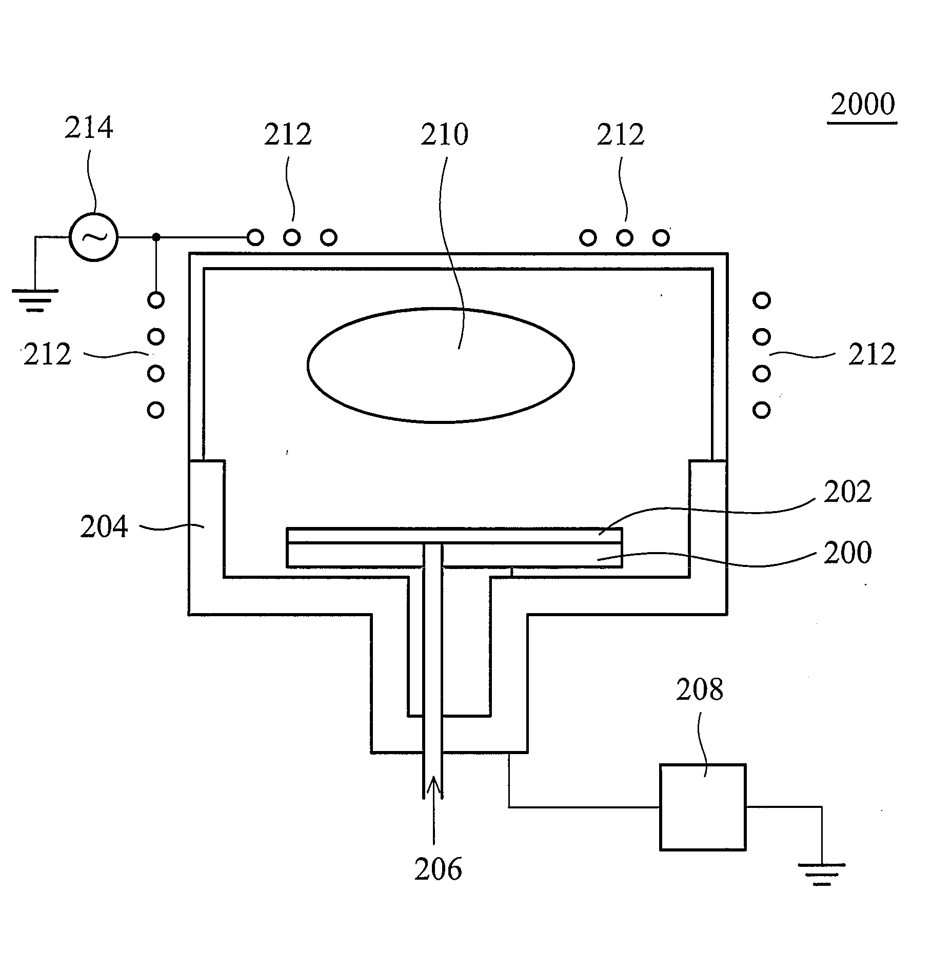
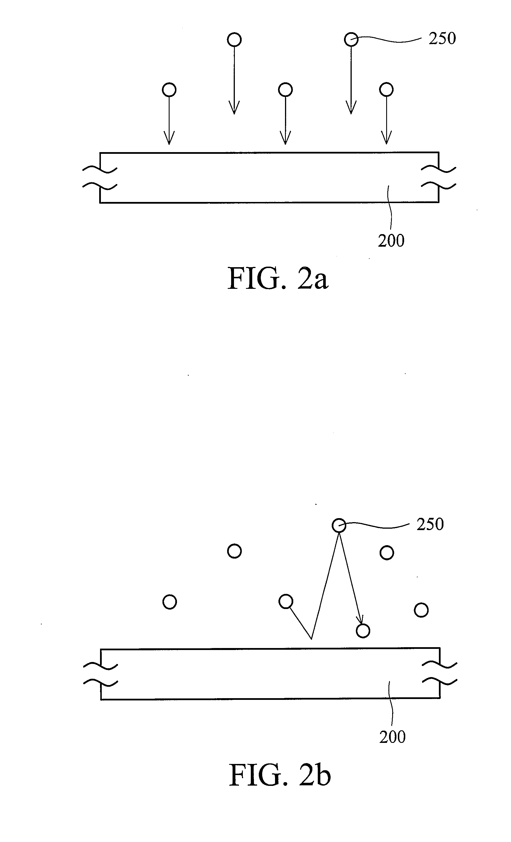
[0025]In this embodiment, the issues described in the exemplary example are addressed through application of RF bias voltage, specifically, via appropriate switching of DC and RF bias voltages during the early process stage (or so-called nuclear formation stage). The application allows avoidance of over bombardment effects during the nuclear formation stage, resulting in obtainment of stable high density plasma. Next, in the propagation stage, DC bias voltage is applied, effectively enhancing the deposition rate and stability of crystalline. It is important to note, that compared to the exemplary example in which only DC bias voltage is employed in the entire process, this embodiment utilizes an integrated bias system to apply different bias voltages at different processing stages. In doing so, the electrical field reversal property of RF bias voltage not only results in extension of mean free path of charged particles in the plasma region, but also reduces bombarding effects of pla...
second embodiment
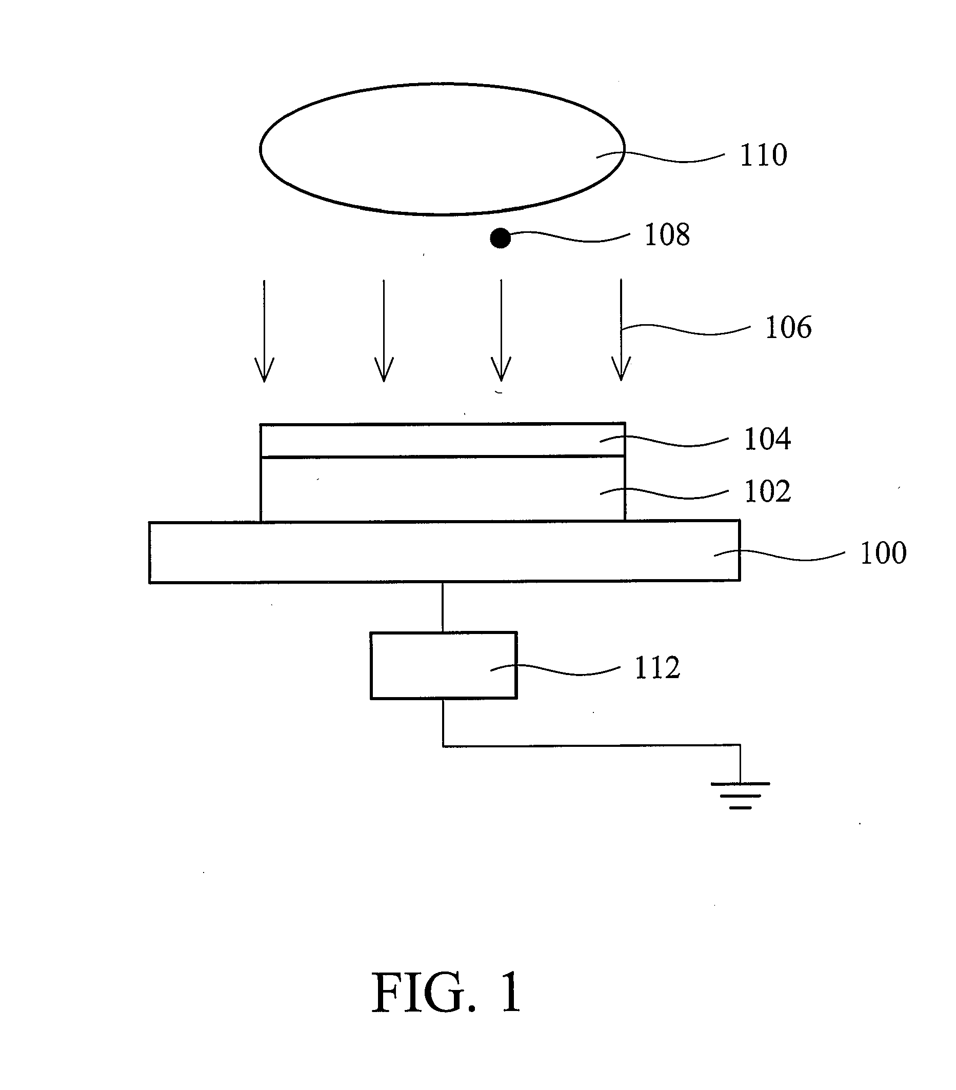
[0034]Referring to FIG. 5, the TFT process of this embodiment features direct formation of a micro-silicon active layer 506 and a micro-silicon doped layer 508 on a substrate with a gate electrode 502 and a gate dielectric layer 504 thereon by method of the previous described first embodiment. Subsequent conventional processes are then performed. Finally, a low temperature polysilicon TFT is obtained.
[0035]In the integrated bias system of this embodiment, energy generated from bombarding of ions is transmitted to atoms on the surface, resulting in diffusion of the atoms on the surface with sufficient energy to active sites. The diffused atoms sequentially form the insulating layer 504, micro-silicon active layer 506 and micro-silicon doped layer 508. When the micro-silicon doped layer 508 is formed on the active layer, a lightly doped junction (not shown) is formed on the interface, without additional ion implantation or thermal processes. In doing so, performance of devices is enha...
PUM
| Property | Measurement | Unit |
|---|---|---|
| temperature | aaaaa | aaaaa |
| bias voltage | aaaaa | aaaaa |
| RF bias voltage | aaaaa | aaaaa |
Abstract
Description
Claims
Application Information
 - R&D
- Intellectual Property
- Life Sciences
- Materials
- Tech Scout
- Unparalleled Data Quality
- Higher Quality Content
- 60% Fewer Hallucinations
Browse by: Latest US Patents, China's latest patents, Technical Efficacy Thesaurus, Application Domain, Technology Topic, Popular Technical Reports.
© 2025 PatSnap. All rights reserved.Legal|Privacy policy|Modern Slavery Act Transparency Statement|Sitemap|About US| Contact US: help@patsnap.com