Mesa-Type Photodetectors With Lateral Diffusion Junctions

a technology of diffusion junctions and pin photodiodes, applied in the field ofmesa-type pin photodiodes, can solve the problems of poor reliability of mesa-based pin pds, inability to pass the stringent telcordia aging test, and inability to include, etc., and achieve the effect of superior reliability

Active Publication Date: 2009-01-22
LUMENTUM OPERATIONS LLC
View PDF23 Cites 19 Cited by
  • Summary
  • Abstract
  • Description
  • Claims
  • Application Information

AI Technical Summary

Benefits of technology

[0013]The present invention has found that without resorting to the complicated regrowth approach, a simple Zn diffusion process can be used to create high-quality semiconductor junction interfaces at the exposed critical surface or to terminate the narrow-bandgap photon absorption layer(s). A key aspect of the invention is to convert the epitaxial material layer(s) near or at the vicinity of the etched mesa trench or etched mesa step(s) into a different dopant type through impurity diffusion process. The resultant lateral diffused p-n junction interface is known to be with much superior reliability than the traditional passivation methods with dielectric film(s) and / or BCB / polyimide, especially for the In(Al)GaAs / InP-based material system, for example.

Problems solved by technology

However, mesa-type photodiodes suffer from poor reliability.
Even though many efforts have been invested in the development of surface-passivation techniques to reduce the surface defects and traps, mesa-based PIN PDs have not yet been able to deliver satisfactory performance to pass the stringent Telcordia aging test.
But this method does not include mesa-type PDs.
The added steps for epitaxial regrowth add significant complexity and expense to photodiode manufacture.
And dielectric coating or BCB alone has proven inconsistent in its ability to reduce dark current, and insufficient to meet data-com and telecom aging requirements.
This is a very complicated structure requiring critical etching and implant steps.
In spite of these efforts, it is believed that the lifetime of this avalanche photodiode is ten times shorter than their standard planar avalanche photodiode and thus not sufficient for telecommunications use.” US application no.

Method used


Image

  • Mesa-Type Photodetectors With Lateral Diffusion Junctions
  • Mesa-Type Photodetectors With Lateral Diffusion Junctions
  • Mesa-Type Photodetectors With Lateral Diffusion Junctions

Examples


Embodiment Construction

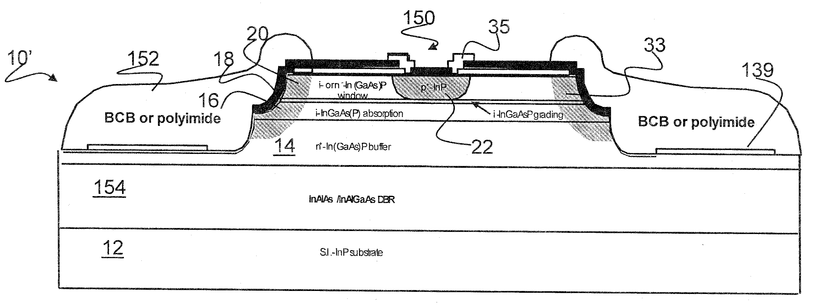
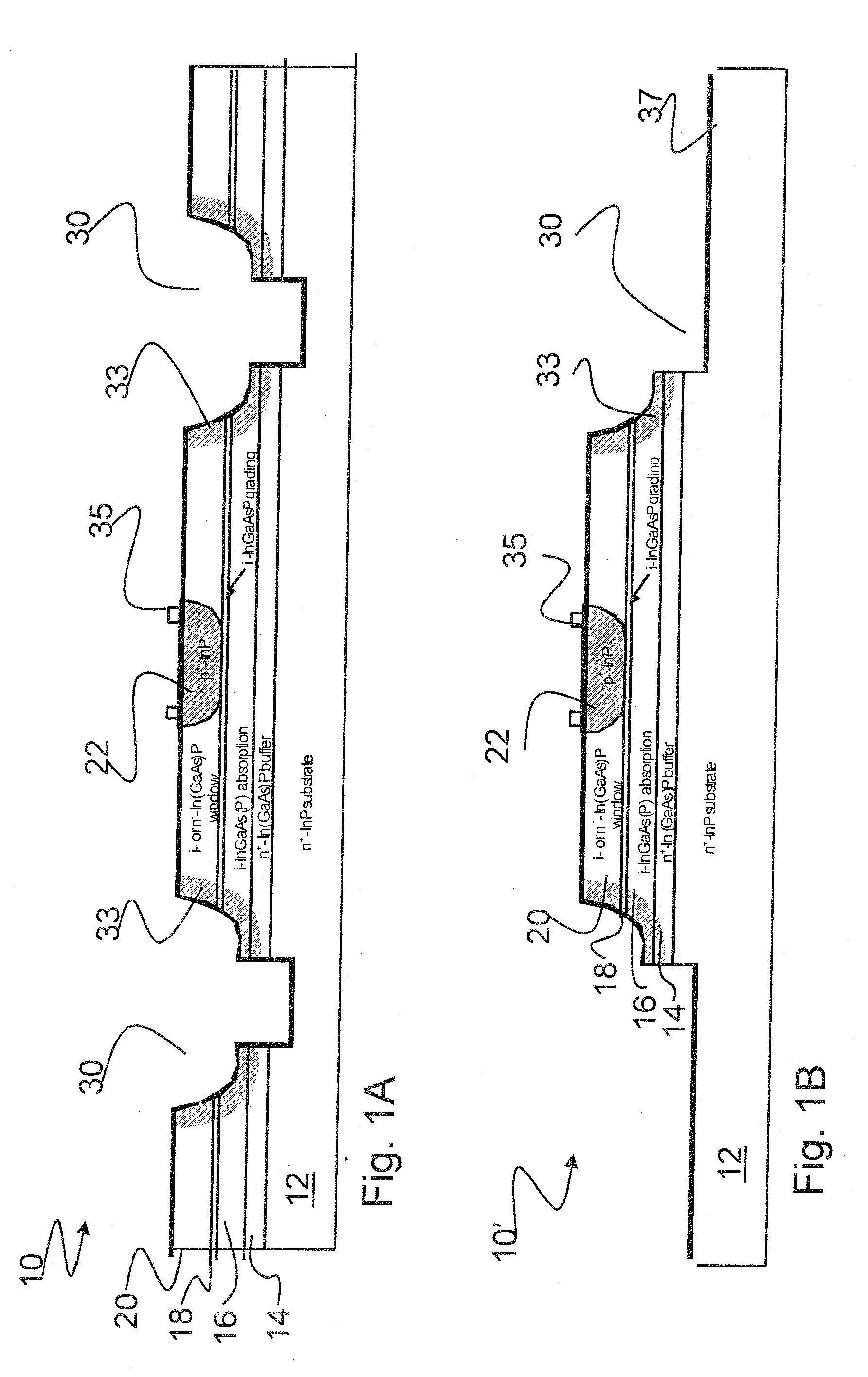
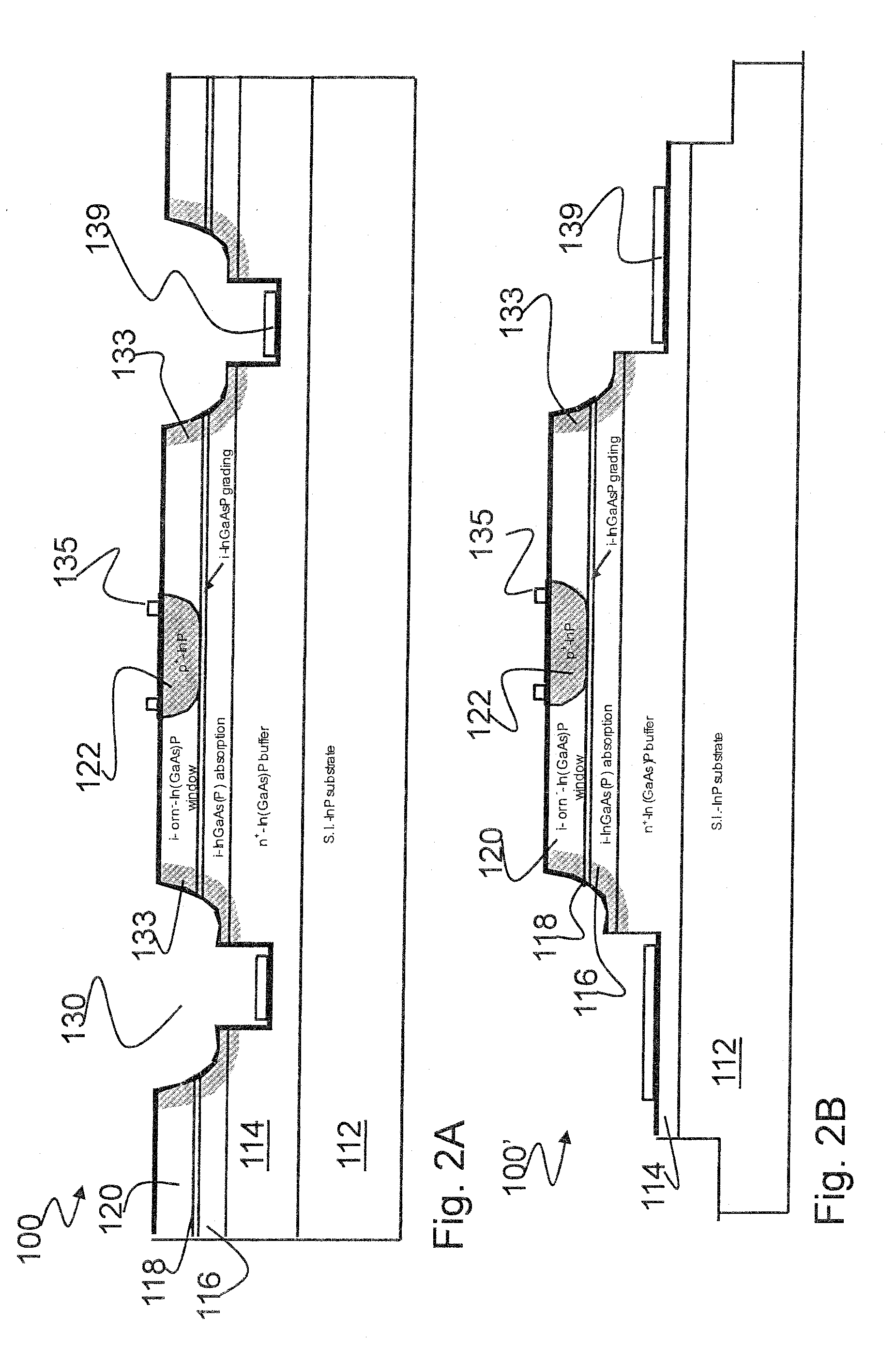
[0034]The present invention provides a mesa-type diffused PIN photodiode as shown by example at 10 in FIG. 1A, which includes a diffused lateral p-n junction 33 to assist in passivation of the sensitive small-bandgap absorption layers. Photodiode 10 includes an epitaxial structure of the following layers: an n+InP substrate 12, an n+InP or InGaAsP buffer layer 14, an intrinsic InGaAs or InGaAsP absorption layer 16, an intrinsic InGaAsP grading layer 18, and an intrinsic or n−InGaAsP or InP window layer 20 with a diffused p-n junction of p+InP active region 22. The mesa is defined by a ring shaped trench 30. Peripheral material beyond the trench 30 is etched away or not depending on the desired bond pad placement (not shown), as is well understood in the art. Photodiode 10 has a single top contact, p contact 35. An n-metal contact (not shown) will be plated on the bottom surface of the substrate 12. FIG. 1B illustrates a similar mesa-type diffused PIN photodiode 10′ in which the peri...


PUM


Abstract

The present invention relates to a stable mesa-type photodetector with lateral diffusion junctions. The invention has found that without resorting to the complicated regrowth approach, a simple Zn diffusion process can be used to create high-quality semiconductor junction interfaces at the exposed critical surface or to terminate the narrow-bandgap photon absorption layers. The invention converts the epi material layers near or at the vicinity of the etched mesa trench or etched mesa steps into a different dopant type through impurity diffusion process. Preferably the diffused surfaces are treated with a subsequent surface passivation. This invention can be applied to both top-illuminating and bottom-illuminating configurations.

Description

CROSS-REFERENCE TO RELATED APPLICATIONS[0001]This application claims priority from U.S. provisional application No. 60 / 950,437 filed Jul. 18, 2007, herein incorporated by reference.TECHNICAL FIELD[0002]The present application relates to a mesa-type PIN photodiode with additional dopant diffusion incorporated within or near the mesa trench to provide termination to the sensitive small-bandgap absorption layers, and to a method for making mesa-type PIN photodiodes to improve the reliability of passivation of the absorption layers.BACKGROUND OF THE INVENTION[0003]Mesa-type photodiodes offer a number of advantages over planar avalanche photodiodes (APD), including reduced capacitance and increased bandwidth. However, mesa-type photodiodes suffer from poor reliability. This is due primarily to the structure which exposes the sensitive narrow bandgap absorption layer to foreign material such as air, SiN or other impurities.[0004]Exposed narrow-bandgap photon absorption layer(s) on the etc...

Claims


Application Information

Patent Timeline
Patent Type & Authority Applications(United States)
IPC IPC(8): H01L31/00H01L21/00
CPCH01L31/105Y02E10/544H01L31/184
Inventor HU, SYN-YEMPAN, ZHONG
Owner LUMENTUM OPERATIONS LLC
Why Eureka
Try Eureka