Electronic component-embedded board and method of manufacturing the same

a technology of electronic components and embedded boards, which is applied in the direction of printed circuit stress/warp reduction, printed circuit details, and non-printed electric components of printed circuits. it can solve problems such as imbalance in the stress applied to the substrate, and achieve the effects of reducing the number of internal stresses

Active Publication Date: 2009-01-29
TDK CORPARATION
View PDF7 Cites 16 Cited by
  • Summary
  • Abstract
  • Description
  • Claims
  • Application Information

AI Technical Summary

Benefits of technology

[0018]In the present manufacturing method, the member is preferably mounted so as to enclose the electronic component. In this manner, by disposing the member in, so to speak, a frame-like arrangement, the linear coefficient of thermal expansion and the mechanical strength of the unmounted portion enclosing the electronic component are averaged without local differences (i.e., without directional anisotropy). As a result, nonuniform internal stress is further alleviated, substrate strength is further enhanced, and warpage of the electronic component-embedded board is further suppressed.
[0019]In addition, the electronic component and the member are preferably mounted on approximately the same plane. Due to such an arrangement, nonuniform internal stress not only in the planar direction of the substrate but also in the thickness direction thereof is more readily alleviated. As a result, warpage of the electronic component-embedded board is more effectively suppressed.
[0020]In this case, the member described above is preferably thinner than the electronic component. Due to such an arrangement, for example, when pressurizing and curing resin to form an insulating layer, resin flows from the peripheral region of the electronic component-mounting portion to the unmounted portion in an easier manner. Consequently, pressure can now be uniformly applied to the electronic component in an easier manner, and the adhesion between the electronic component and the insulating layer as well as the evenness of the thickness of the electronic component-embedded board and the flatness thereof can be improved. Additionally, in this case, the efficient removal of bubbles that may exist or may be incorporated between the above-described member, wiring layer, insulating layer, electronic component and the like enables suppression of occurrences of manufacturing/processing problems. As a result, process yield and mounting reliability can be improved.
[0021]Furthermore, with the member described above, it is preferable that the spatial volume ratio occupied by the element within the insulating layer continuously or incrementally decreases in a direction towards the outer pe...

Problems solved by technology

Extensive research carried out by the present inventors in order to solve the problems described above revealed that degrees (levels) of thermal expansion and thermal contraction caused by heat applied during the formation of an insulation layer or the like differ between an electronic component-mounting portion (a region of a...

Method used


Image

  • Electronic component-embedded board and method of manufacturing the same
  • Electronic component-embedded board and method of manufacturing the same
  • Electronic component-embedded board and method of manufacturing the same

Examples


first embodiment

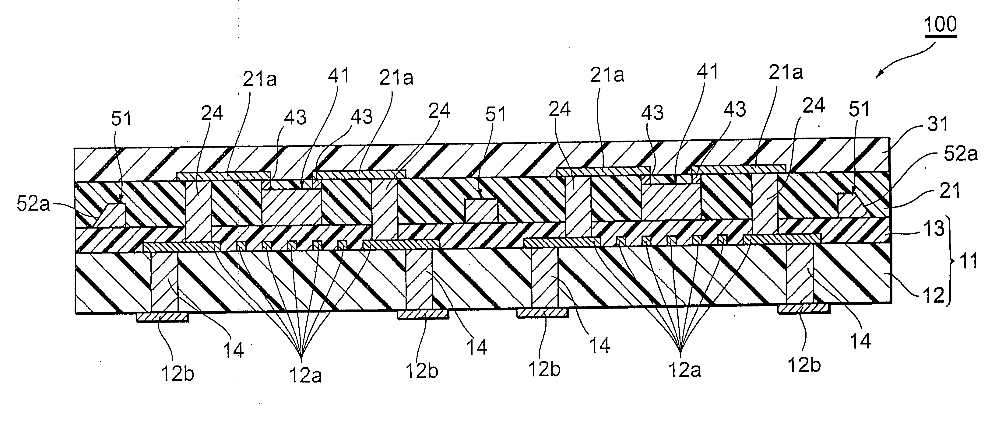
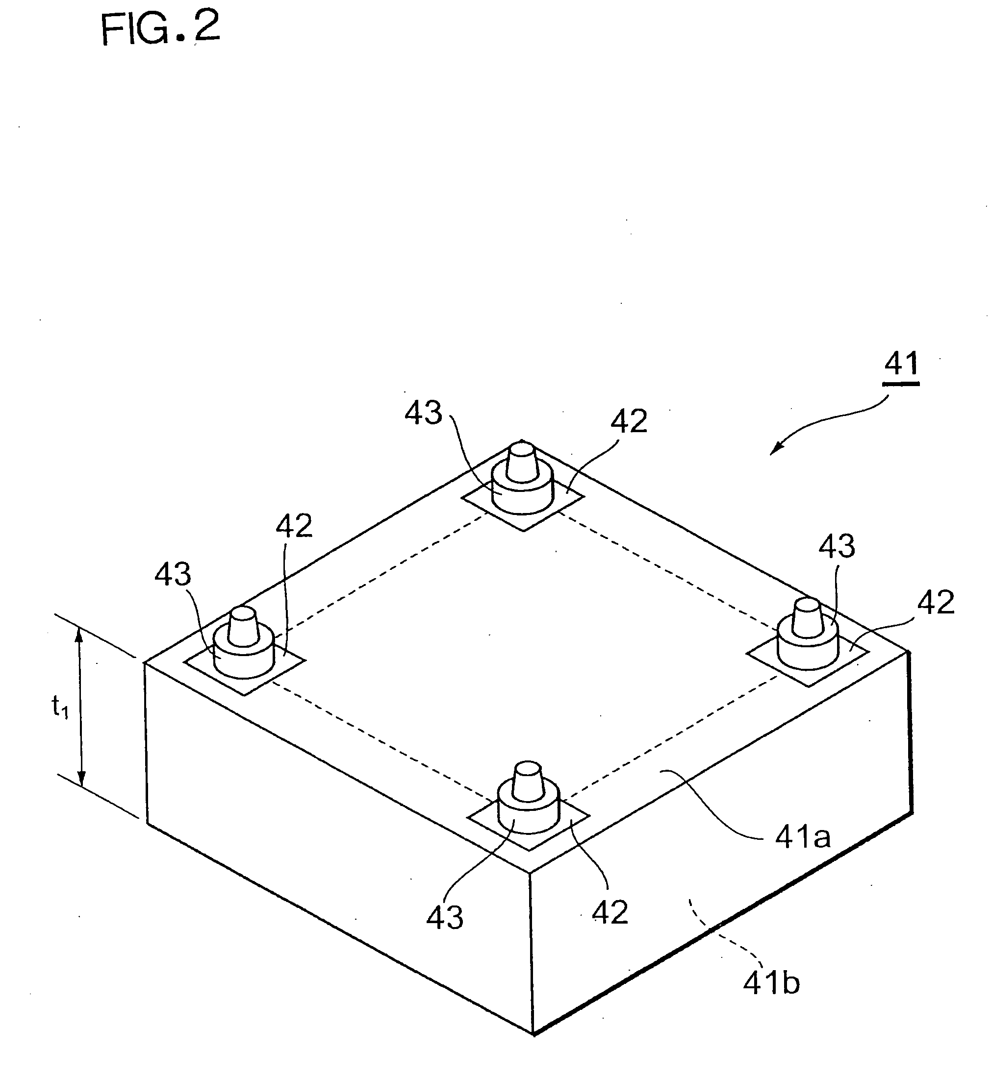
[0045]FIG. 1 is a schematic cross-sectional diagram showing substantial parts of a first embodiment of an electronic component-embedded board according to the present invention. A worksheet 100 is an electronic component-embedded assembly substrate that contains, within a sheet plane thereof, a total of four individual substrates arranged in a two-by-two grid, and includes insulating layers 21 and 31 on one surface (the shown upper surface) of an approximately rectangular substrate 11, and electronic components 41 and plate-like frame member (member) 51 embedded at predetermined positions inside the insulating layer 21.

[0046]The substrate 11 includes wiring layers (patterns) 12a and 12b formed on both faces of the insulating layer 12, and an insulating layer 13 laminated on top of the wiring layer 12a by vacuum pressure-bonding an insulating resin film on the wiring layer 12a. The wiring layer 12a and the wiring layer 12b are electrically connected to each other via a via 14 penetra...

second embodiment

[0074]FIG. 17 is a plan view showing a schematic configuration of a second embodiment of an electronic component-embedded board according to the present invention. A worksheet 300 is configured similar to the worksheet 100 according to the first embodiment described above, expect that a member 81 satisfying formula (1) above is provided in place of the plate-like frame member 51. The member 81 is constituted by plate members 82 having a rectangular cross-section and a cross-like plate member 83 having a rectangular cross-section and, as shown, a plurality of plate members 82 are disposed in a frame-like arrangement in a peripheral edge portion of the substrate 11 and the cross-like plate member 83 is disposed inside the frame. In addition, the plate members 82 are thinner than the plate member 83.

[0075]Operations and effects similar to those of the first embodiment described above can be achieved also using the member 81 described above. In addition, since the member 81 is separatel...

third embodiment

[0076]FIGS. 18 and 19 are, respectively, a plan view and a partially cross-sectional view showing a schematic configuration of a third embodiment of an electronic component-embedded board according to the present invention. A worksheet 400 is configured similar to the worksheet 100 according to the first embodiment described above, expect that a member 84 satisfying formula (1) above is provided in place of the plate-like frame member 51. The member 84 is constituted by a frame member 85 in which a plurality of various through-holes (recesses) 85b are formed on a roughened surface 85a, and plate members 86 having a rectangular cross section, and as shown, the plate members 86 are disposed within the frame that is the frame member 85. For brevity, the through-holes 85b are not shown in FIG. 18. The through-holes 85b provided on the surface 85a of the frame member 85 are disposed so that volumes of the recesses (inner volumes) increase in a direction towards the outer periphery of the...


PUM

PropertyMeasurementUnit
Efficiencyaaaaaaaaaa
Volume ratioaaaaaaaaaa
Thermal expansion coefficientaaaaaaaaaa

Abstract

A method of manufacturing an electronic component-embedded board is provided which is capable of suppressing warpage without requiring complicated processes at low cost and which offers high productivity and economic efficiency. A worksheet 100 includes insulating layers 21 and 31 on one surface of an approximately rectangular substrate 11, and an electronic component 41 and a plate-like frame member (member) 51 embedded inside the insulating layer 21, wherein the plate-like frame member 51 satisfying the relationship represented by the following formula (1): α1<α3 and α2<α3 . . . (1), is mounted on an unmounted portion of the electronic component 41 on the substrate 11. In the formula, α1, α2 and α3 respectively denote the linear coefficients of thermal expansion (ppm/K) of the electronic component 41, the plate-like frame member 51, and the substrate 11, the respective wiring layers or the respective insulating layers.

Description

BACKGROUND OF THE INVENTION[0001]1. Field of the Invention[0002]The present invention relates to an electronic component-embedded board and a method of manufacturing the same.[0003]2. Description of the Related Art[0004]In recent years, with the progress in electronics technology, there has been a growing demand towards higher density in printed circuit boards. As such, multilayer printed circuit boards in which are laminated pluralities of wiring patterns and insulating layers are becoming widely used.[0005]Conventionally, for the purpose of increasing productivity, printed circuit boards used in these types of applications are manufactured in a “multiple dice from one substrate” manner in which, for example, an approximately 300 mm to 500 mm square worksheet (assembly substrate) provided with a plurality of wiring pattern groups (wiring layers) for printed circuit boards is separated into individual dice by dicing or the like to obtain a plurality of printed circuit boards (indivi...

Claims


Application Information

Patent Timeline
IPC IPC(8): H05K3/30H05K1/16
CPCH01L23/5389Y10T29/49146H01L24/82H01L24/97H01L25/0655H01L2224/18H01L2224/97H01L2924/01003H01L2924/01012H01L2924/01013H01L2924/01015H01L2924/0102H01L2924/01029H01L2924/0103H01L2924/01033H01L2924/01038H01L2924/0104H01L2924/01042H01L2924/01047H01L2924/01057H01L2924/01073H01L2924/01074H01L2924/01078H01L2924/01079H01L2924/01082H01L2924/04953H01L2924/14H01L2924/19041H01L2924/19042H01L2924/19043H05K1/0271H05K1/185H05K3/0052H05K3/0097H05K3/4602H05K2201/068H05K2201/2009H05K2203/0169H01L24/18H01L2924/014H01L2924/01006H01L2924/01019H01L2924/01024H01L2224/82H01L2924/12042H01L2924/3511H01L2224/04105H01L2224/16227H01L2224/73267H01L2224/92244H01L24/19H01L2924/00
Inventor KANEMARU, YOSHIKAZUMORITA, TAKAAKIKAWABATA, KENICHI
Owner TDK CORPARATION
Why Eureka
Try Eureka