Electrolyte pattern and method for manufacturing an electrolyte pattern

Inactive Publication Date: 2009-02-12
SEIKO EPSON CORP
8 Cites 41 Cited by

AI-Extracted Technical Summary

Problems solved by technology

A major disadvantage of ECTs is the fact that, in comparison to OFETs, their switching times are very long.
Two major problems with electrolyte-gated transistors are their low operation frequencies and the occurrence of hysteresis during switching.
In the case of ECTs, an additional factor limiting the switching speed is the rate of diffusion of counter-ions into the bulk of the semiconductor material in the transistor channel.
A contributing factor to the occurrence of hysteresis during switching of both electrolyte-gated FETs and ECTs is the transient inhomogeneity of the electric field along the width of the transistor channel when a laterally positioned gate electrode is used.
Another problem with electrolyte-gated transistors is the leakage and diffusion of ions from the electrolyte into other device components.
The performance of electric field-driven devices ...

Method used

[0085]The source, drain, and gate electrodes 2, 3, 4 are preferably made from an electrochemically inert material such as gold, platinum, palladium or a conductive form of carbon, in order to prevent electrochemical corrosion during operation whilst in contact with the electrolyte.
[0104]When inkjet printing is used to deposit the etch mask 7, the material for the etch mask 7 must be formulated into an ink that is printable onto the gelling agent layer 6. This requires an appropriated choice of solvents and material concentrations (resulting in an appropriate viscosity and surface tension) in order to enable good ink ejection, wetting of the surface of the gelling agent layer 6, and drying.
[0112]One purpose of the bank 8 is to prevent leakage by enclosing the electrolyte 10, which is particularly important where the electrolyte 10 is a liquid. The bank 8 also prevents diffusion of ions from the electrolyte 10 to other device components.
[0113]Another purpose of the bank 8 is to enclose volatile components of the electrolyte 10 such as water (in the case of water-based electrolytes), or organic solvents (in the case of organic solvent-based electrolytes) in order to prevent the electrolyte 10 drying out, thereby maintaining the ionic conductivity of the electrolyte 10 at a constant level.
[0115]The bank material 8 should therefore be insoluble in the electrolyte 10 and non-polar in order to prevent ion diffusion. The bank material 8 should also have extremely small diffusion coefficients for ions and water molecules. Possible bank materials include the fluoropolymer Cytop (supplied by Asahi Glass Inc., Japan) and the cycloolefin copolymer Zeonex (supplied by Zeon Corporation, Japan). Both Cytop and Zeonex are chemically resistant, display small dielectric constants (2.1 and 2.2-2.3, respectively), and absorb less than 0.01% water.
[0133]Conversely, in the case of a PIL-FET having an n-type transistor channel, the electrolyte 10 must not comprise any mobile protons or other cations in order to prevent the electrochemical reduction of the semiconductor 5 in the transistor channel. Therefore, PIL-FETs having n-type transistor channels require an electrolyte 10 comprising immobile, polymeric cations in combination with mobile anions.
[0141]Thus, in order to maintain charge neutrality within the electrolyte in an ECT, the gate electrode in the transistor either has to release an equivalent amount of anions or electrons into the electrolyte, or remove an equivalent amount of cations from the electrolyte. This exchange of ions between the semiconductor layer in the transistor channel and the electrolyte in ECTs therefore requires a complementary (i.e. opposite) redox reaction to occur at the gate electrode. Specifically, when a ...

Benefits of technology

[0039]Due to the use of a gel electrolyte pattern and the presence of the bank layer in the transistor described above, the risk of the electrolyte leaking and causing damage to other nearby components is greatly reduced. The use of a gel electrolyte pattern also allows other layers such as a gate electrode to be deposited on top of the electrolyte layer without the risk of creating short circuits with the semiconductor in the transistor channel. In addition, since the transistor structure of the present invention has a gel electrolyte layer confined to a window in a bank layer, i.e. a gel electrolyte ...

Abstract

A method for manufacturing a gel electrolyte pattern is disclosed, the method comprising depositing an electrolyte precursor by inkjet printing onto a gelling agent layer. A gel electrolyte pattern is also disclosed, the gel electrolyte pattern comprising either a mixture of a gelling agent and an electrolyte precursor or the products of a chemical reaction between a gelling agent and an electrolyte precursor.

Application Domain

Technology Topic

Image

  • Electrolyte pattern and method for manufacturing an electrolyte pattern
  • Electrolyte pattern and method for manufacturing an electrolyte pattern
  • Electrolyte pattern and method for manufacturing an electrolyte pattern

Examples

  • Experimental program(1)

Example

EXAMPLE
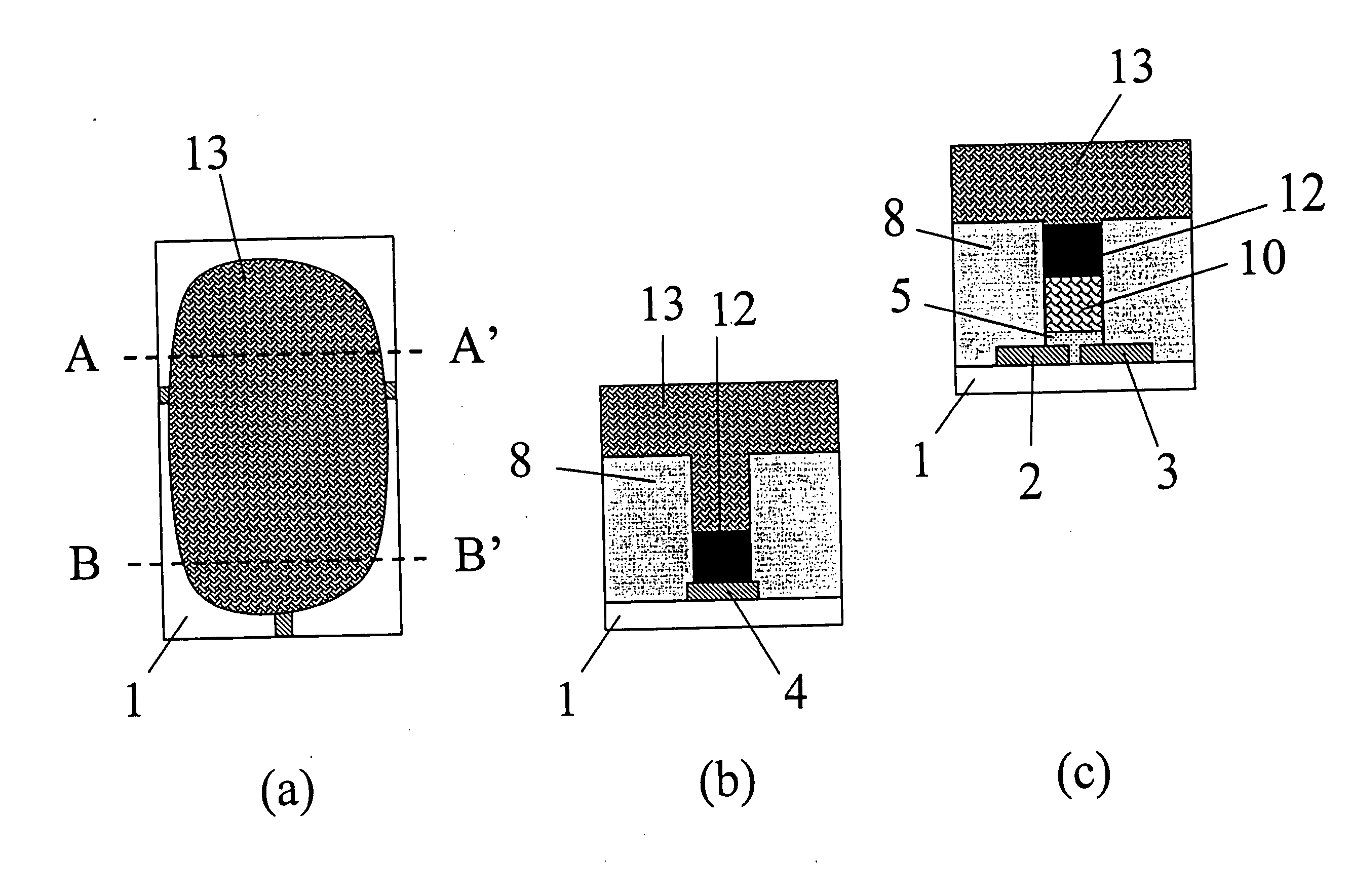
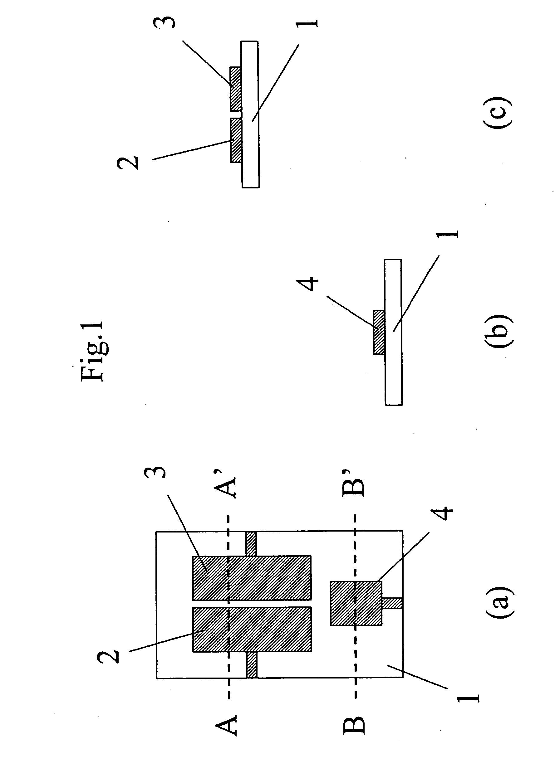
[0147]The following is a preferred embodiment of the manufacturing method and the resulting transistor according to the present invention. In a first step, source, drain, and gate electrodes are patterned from an evaporated gold layer on a glass substrate. The source and drain electrodes are separated so as to define a transistor channel between them. The channel length L is 20 μm, and the width W is 1 mm. The gate electrode is positioned laterally to the source-drain electrode pair, at a distance of 1 mm.
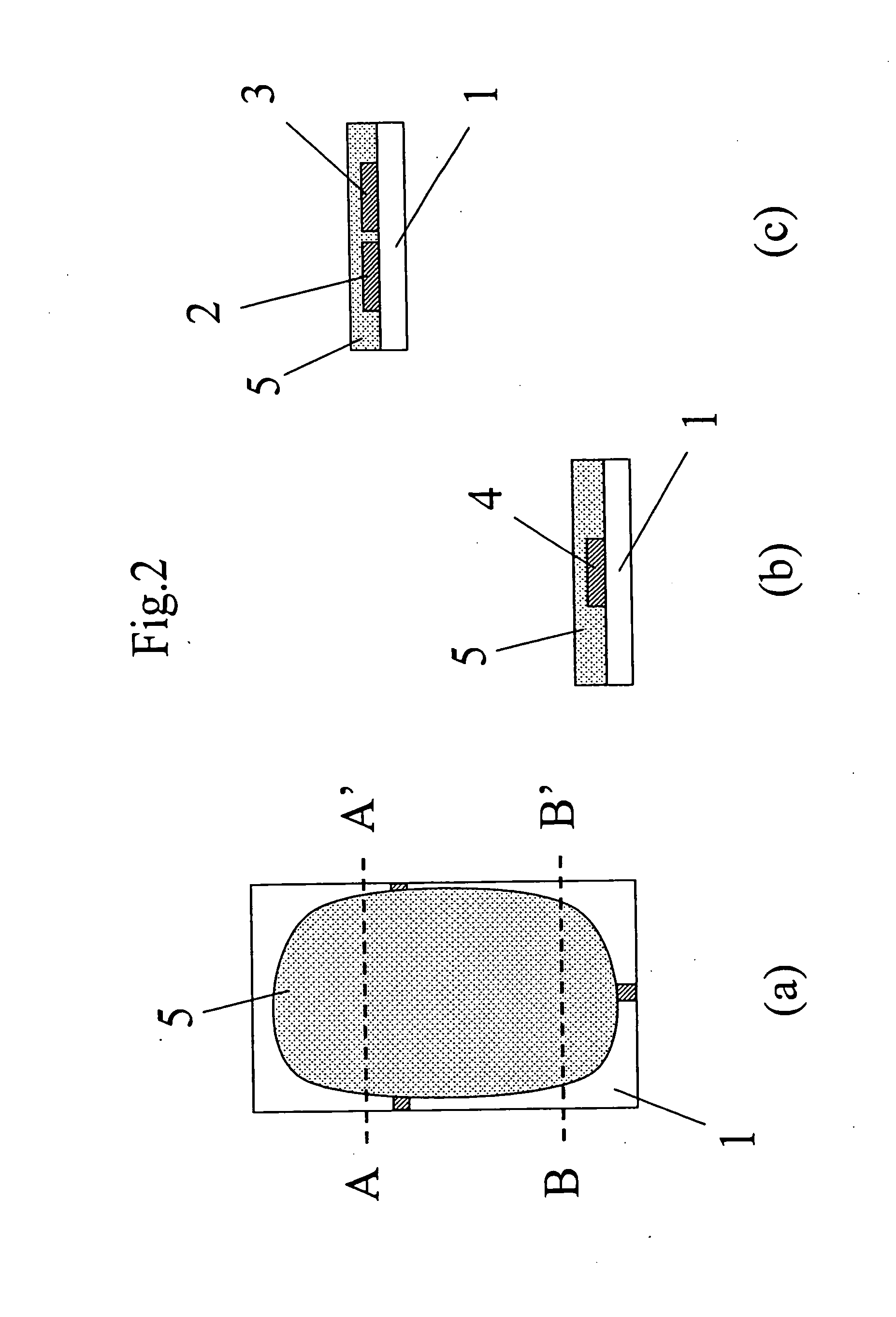
[0148]A thin layer (40 nm thick) of the semiconducting polymer ADS2008 (supplied by American Dye Source Inc., Canada) is then spin-coated onto the substrate from a 1% toluene solution and annealed in air. Annealing is performed at a temperature of 80 deg. C. for 10 minutes.
[0149]A layer (600 nm thick) of the gelling agent poly(methylmethacrylate) (PMMA) is spin-coated onto the semiconductor layer from a 6% butylacetate solution and annealed in air. Again, annealing is performed at a temperature of 80 deg. C. for 10 minutes.
[0150]An etch mask pattern consisting of the fluoropolymer Cytop is inkjet printed onto the PMMA gelling layer, on top of the transistor channel. The Cytop ink comprises Cytop dissolved in a mixture of perfluorotributylamine, FC-70 (supplied by Fluorochem Ltd., UK), and FC-75 (supplied by Fluorochem Ltd., UK). The resulting layer thickness of the etch mask depends on the Cytop concentration in the ink, the droplet spacing, and the number of inkjet printing passes. A layer thickness of at least 200 nm of Cytop is formed over the centre of the transistor channel in this embodiment, in order to provide a reliable etch mask for the ensuing oxygen plasma patterning step.
[0151]An oxygen plasma treatment is then performed to pattern the gelling agent layer and the semiconductor layer. The PMMA gelling agent layer and the ADS2008 semiconductor layer are removed everywhere, except in those areas that are covered by the inkjet printed Cytop etch mask.
[0152]A thick layer of Cytop bank material is spin-coated onto the substrate, covering the source, drain, and gate electrodes and the Cytop/PMMA/ADS2008 multilayered patterns. The thickness of the bank material determines the depth of the resulting bank structure and can be increased by multiple spin-coating steps in combination with intermediate annealing sequences. There is no need to remove the Cytop etch mask from the multilayer patterns prior to the deposition of the Cytop bank layer, as the etch mask material will be removed during the ensuing patterning of the thick Cytop bank layer by inkjet etching.
[0153]The Cytop bank layer is then patterned by inkjet etching. Droplets of a suitable solvent mixture are deposited in multiple passes along a line stretching from the gate electrode over the transistor channel defined by the source and drain electrodes. The number of passes required depends on the thickness of the Cytop bank layer. Inkjet etching in this embodiment is performed using a perfluorinated solvent such as perfluorotributylamine, 3M Fluorinert FC-75, or 3M Fluorinert FC-70. The resulting opening in the bank structure exposes the bi-layer pattern comprising the PMMA gelling layer and the ADS2008 semiconductor on top of the transistor channel, and also exposes a part of the gold gate electrode.
[0154]Next, an electrolyte precursor comprising a 10% vol/vol mixture of ethyl-methyl-imidazolium bis(trifluoromethyl)sulfonylimide (EMI-TFSI; supplied by Toyo Gosei Inc., Japan) in benzylalcohol is inkjet printed onto the PMMA gelling agent pattern via the opening in the bank structure.
[0155]Following printing of the electrolyte precursor, the electrolyte precursor interacts with the gelling agent. Initially, the benzylalcohol component in the electrolyte precursor dissolves the PMMA gelling agent. Then, the evaporation of the benzylalcohol component of the electrolyte precursor results in the formation of a pattern of EMI-TFSI/PMMA gel on top of the ADS2008 semiconductor pattern.
[0156]A gate electrode extension is then formed by inkjet printing a polyaniline emeraldine salt solution in an aromatic solvent on top of the gate electrode and along the opening in the Cytop bank to completely cover the EMI-TFSI/PMMA gel pattern.
[0157]The transistor is completed by spin-coating a thick Cytop encapsulation layer onto the device so as to cover the bank structure and the gate electrode extension.
[0158]The method according to the present invention allows a gel electrolyte pattern to be formed by inkjet printing a liquid material, which is much easier than depositing a gel material directly. In addition to preventing leakage, the gelling of the electrolyte allows other layers such as a gate electrode to be deposited on top of the electrolyte layer without the risk of creating short circuits with layers beneath the gel electrolyte pattern.
[0159]The gel electrolyte patterns according to the present invention can be manufactured simply by depositing an electrolyte precursor, which is typically a liquid material, onto a gelling agent. This process is easier to perform than a process involving depositing a gel electrolyte directly, particularly when used in the manufacture of a device such as an electrochemical transistor or an electrochromic display.
[0160]The preferred embodiment of the invention provides a structure for electrolyte-gated transistors in which the electrolyte layer is sandwiched vertically between the transistor channel and a top-gate electrode extension. In such a device structure, the distance between the extended gate electrode and the transistor channel is minimized, which maximizes the ionic conductance between the transistor channel and the gate electrode. The structure thereby provides fast switching speeds and reduced hysteresis. The transistor structure of the invention is suitable for being manufactured using inkjet printing and other solution-based processes, which allows the transistor according to the invention to be fabricated reliably, quickly and inexpensively. Furthermore, the invention provides a manufacturing method for producing the transistor structure. The method according to the invention provides a reliable and quick manufacturing process for an electrolyte-gated transistor.
[0161]Furthermore, the invention provides a combination of a bank structure and an encapsulation layer, which efficiently contains the electrolyte of the transistor and prevents the diffusion of ions out of the electrolyte.
[0162]In addition to enclosing the electrolyte within the bank structure and the encapsulation layer, the transistor structure of the invention prevents leakage of the electrolyte by providing a pattern of gelled, rather than liquid, electrolyte. By using a gelling agent layer and a separate electrolyte precursor that interacts with the gelling agent layer, the method of the invention allows a gelled electrolyte to be formed using solution processes, in particular inkjet printing.
[0163]Another effect of the gelling of the electrolyte is to allow a gate electrode extension to be printed onto the top surface of the electrolyte pattern without the risk of creating a short circuit with the semiconductor in the transistor channel below the electrolyte.
[0164]Finally, the invention allows a constant ionic conductivity to be maintained in the electrolyte of the transistor by preventing both the loss of water or volatile organic solvents from the electrolyte due to evaporation, and the absorption of water from the environment by the electrolyte. The invention avoids these problems because both the bank structure and the encapsulation layer are chosen to comprise barrier materials with extremely low diffusion coefficients for water and/or organic solvent molecules.
[0165]The aforegoing description has been given by way of example only and it will be appreciated by a person skilled in the art that modifications can be made without departing from the scope of the present invention.
[0166]In particular, while the method and the gel electrolyte pattern of the present invention have been described in the context of a transistor, the present invention can be applied equally to any other device using an electrolyte, for example an electrochromic display.

PUM

no PUM

Description & Claims & Application Information

We can also present the details of the Description, Claims and Application information to help users get a comprehensive understanding of the technical details of the patent, such as background art, summary of invention, brief description of drawings, description of embodiments, and other original content. On the other hand, users can also determine the specific scope of protection of the technology through the list of claims; as well as understand the changes in the life cycle of the technology with the presentation of the patent timeline. Login to view more.

Similar technology patents

Wear assembly for the digging edge of an excavator

ActiveUS6986216B2Easily modifyReduce riskPower reduction by energy recoveryPower reduction by adiabatic operationEngineeringExcavator
Owner:ESCO GRP LLC

Classification and recommendation of technical efficacy words

Why Eureka
Try Eureka