Multilayer printed circuit board
- Summary
- Abstract
- Description
- Claims
- Application Information
AI Technical Summary
Problems solved by technology
Method used
Image

Examples
Embodiment Construction
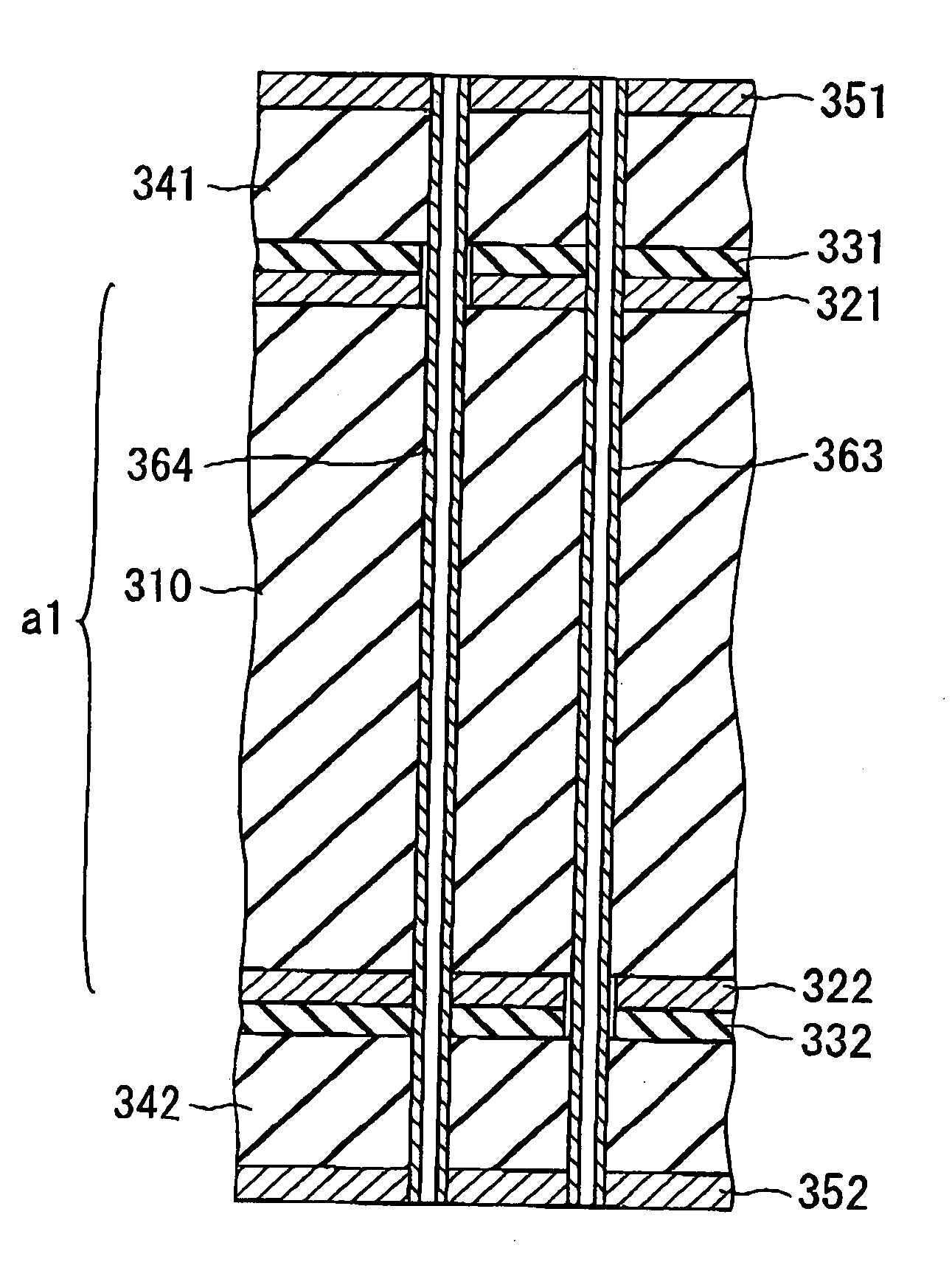
[0022]The present inventor have studied the problem of JP-A 2006-100608 or JP-A 2006-019590 and have found out the cause of the problem. First explanation will be made about the cause of the problem.
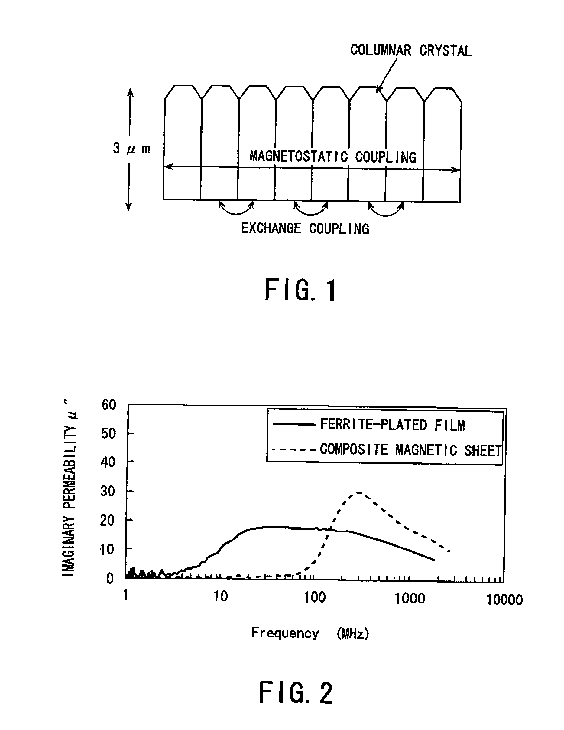
[0023]In general, when a noise suppression member or material is disposed directly on a transmission line such as a signal pattern formed on a printed circuit board, its noise suppression effect is represented by the following formula (1):
PlossPin∝M·μ″·f·δ,(1)
where Ploss / Pin shows noise suppression effect per unit line length, M is coupling coefficient between the noise suppression member and high-frequency magnetic flux caused by a current flowing the transmission line, and δ is a thickness of the noise suppression member.
[0024]Coupling coefficient M is influenced by a clearance between the noise suppression member and the transmission line; a large clearance may remarkably deteriorate the coupling coefficient M. Therefore, removal of the clearance is required to obtain a large noise su...
PUM
| Property | Measurement | Unit |
|---|---|---|
| Length | aaaaa | aaaaa |
| Electrical resistivity | aaaaa | aaaaa |
| Fraction | aaaaa | aaaaa |
Abstract
Description
Claims
Application Information
 - R&D Engineer
- R&D Manager
- IP Professional
- Industry Leading Data Capabilities
- Powerful AI technology
- Patent DNA Extraction
Browse by: Latest US Patents, China's latest patents, Technical Efficacy Thesaurus, Application Domain, Technology Topic.
© 2024 PatSnap. All rights reserved.Legal|Privacy policy|Modern Slavery Act Transparency Statement|Sitemap