
Textured substrate for epitaxial film formation and surface improving method of textured substrate for epitaxial film formation

a technology of epitaxial film and textured substrate, which is applied in the direction of crystal growth process, record information storage, superconductor devices, etc., can solve the problems of difficult to improve the orientation degree no matter, and more improvement was considered difficult, so as to improve the orientation degree, and improve the effect of substrate orientation

Active Publication Date: 2009-02-26
TANAKA PRECIOUS METAL IND
View PDF4 Cites 17 Cited by
  • Summary
  • Abstract
  • Description
  • Claims
  • Application Information

AI Technical Summary

Benefits of technology

[0007]Further, in the textured substrate, it is common to form the textured metal layer by subjecting a plate material (foil material) such as copper to cold working or hot processing and heat treatment so as to be re-crystallized. By such cold working and heat treatment, the orientation degree Δφ of the textured metal can be improved. Being different depending on the kind of constituent metals, the orientation degree Δφ of copper relatively easily textured is approximately 5°, and the orientation degrees Δφ of nickel and silver can be increased up to the extent of 6° and 9°.
[0009]Any of the orientation degrees Δφ and Δω of the textured metal layer affects an orientation degree of the epitaxial thin film formed on the metal layer, and eventually, determines the property of the epitaxial thin film. Even slight improving in these orientation degrees facilitates the practical use of epitaxial growth materials such as superconducting materials.
[0010]Hence, an object of the present invention in the textured substrate for epitaxial thin film growth is to provide a more improved orientation degree of the surface and an improving method of an orientation degree of the oriented substrate, and to provide a textured substrate capable of manufacturing an epitaxial thin film having a more excellent characteristic than heretofore.
[0023]The manufacturing method of the textured substrate for epitaxial film formation according to the present invention, that is, the surface improving method for improving crystal orientation of the textured metal layer allows a metal thin film of 1 to 5000 nm in thickness to be epitaxially grown on the surface of the textured metal layer of the textured substrate.
[0031]As described above, the textured substrate for the epitaxial film formation according to the present invention has further improved the orientation degree of the substrate which has been improved in orientation degree to the fullest extent by the conventional method. Further, the surface roughness thereof is regulated by nano-order, so that a high quality epitaxial film having a high crystal orientation and exerting an expected characteristic can be formed. The epitaxial film formed by using the present invention is not particularly limited if formed by the epitaxial growth, and for example, can be suitably used for an oxidative superconducting conductor, and can form a good superconducting conductor layer excellent in crystal orientation.

Problems solved by technology

However, the improvement of the orientation degree Δφ is restricted to the above described values even if the working condition and the heat treatment condition were adjusted, and more improvement was deemed difficult.
Further, though the orientation degree Δφ is adjustable, it was deemed difficult to improve the orientation degree Δω no matter how the working condition and the heat treatment condition were adjusted.

Method used


Image

  • Textured substrate for epitaxial film formation and surface improving method of textured substrate for epitaxial film formation

Examples


first embodiment

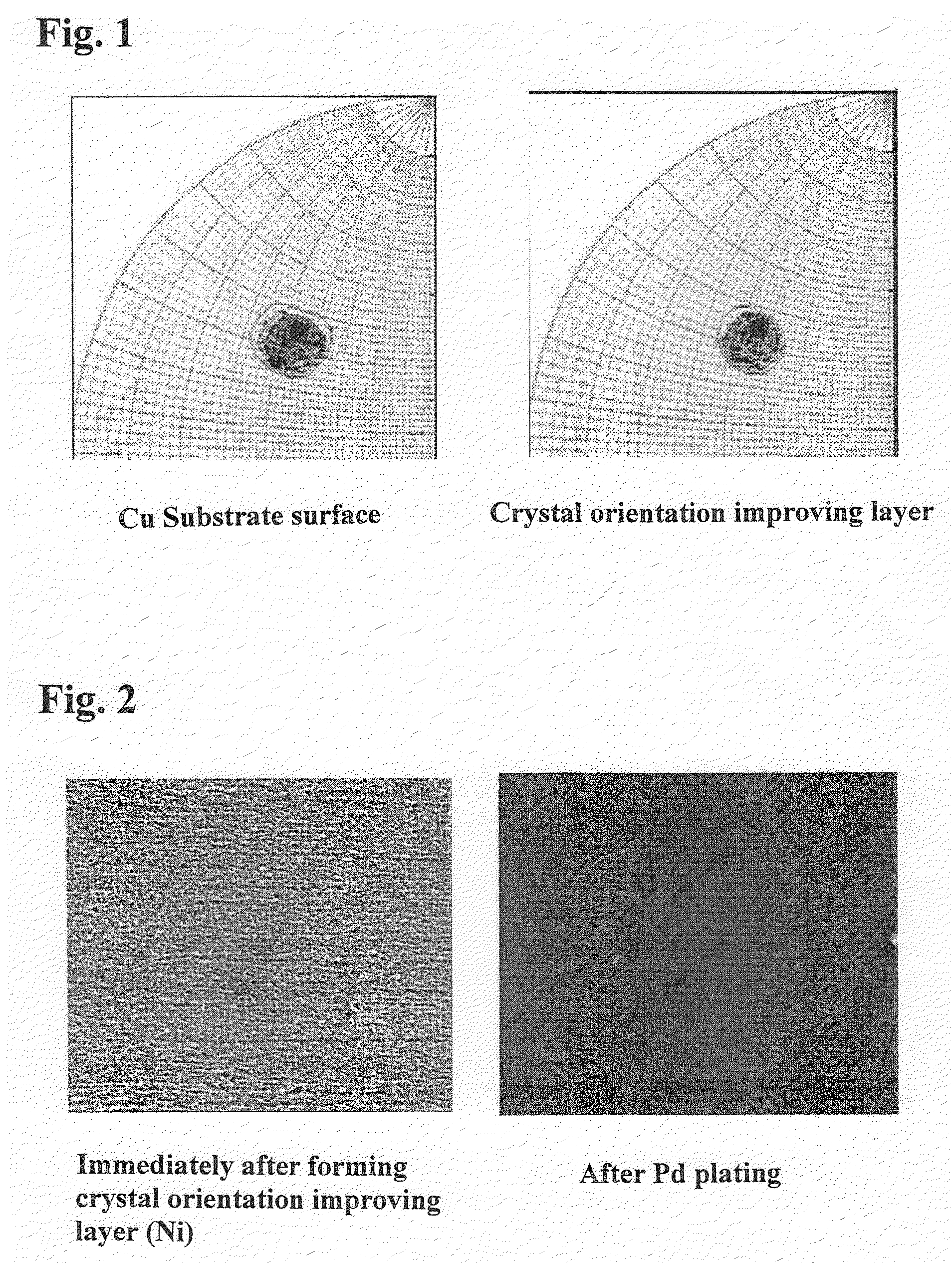
Formation and Study of Crystal Orientation Improving Layer

[0035]First, a tape-shaped copper plate of 1000 μm in plate thickness was prepared, and this copper plate was set to a reduction ratio of 95% by rolling, and was cold-rolled at room temperature and made into a tape material of 50 μm. After rolling, the copper tape was subjected to a heat treatment, so that the crystal was textured. This heat treatment was performed by heating at the temperature of 750° C. for two hours in the atmosphere made of a nitrogen gas 95% and a hydrogen gas 5%.

[0036]The copper substrate subjected to the above described orientation process was plated with nickel as a crystal orientation improving layer. When plated with nickel, the substrate was subjected to acid degreasing and electrolytic degreasing, and subsequently was subjected to electrolytic plating in a nickel plating bath (watt bath). The plating conditions were temperature of 40° C. and current density of 1 A / dm2, and the film thickness was a...

second embodiment

[0043]Here, based on the similar copper substrate to the first embodiment, other metals (Ag and Au) were formed as orientation improving layers, while changing the thickness thereof. The result is shown in Table 2.

TABLE 3ConfigurationΔωSubstrateImproving LayerΔφTDRDEx. 8CuAg (500 nm)4.65°5.38°4.97°Ex. 9Ag (1000 nm)4.62°5.26°4.83°Ex. 10Au (500 nm)4.72°5.44°5.10°Ex. 11Au (1000 nm)4.69°5.35°5.00°Com. Ex. 1—5.17°7.46°5.87°

[0044]Similarly to the first embodiment, an effect of the improvement of smoothness by plating with a slight amount of metal was studied. The result is shown in Table 4.

TABLE 4ConfigurationSubstrate / ImprovingAddedSurfaceΔωlayermetal *roughnessΔφTDRDEx. 8Cu / Ag—21 nm4.65°5.38°4.97°Ex. 12(500 nm)Pd (5 nm)11 nm4.89°5.03°5.24°Ex. 10Cu / Au—20 nm4.72°5.44°5.10°Ex. 13(500 nm)Pd (5 nm)16 nm4.75°4.79°4.98°* Numerical values in parentheses are added amounts equivalent to film thickness

[0045]From Table 3, an effect of the improvement of the orientation degrees Δφ and Δω was seen ev...

third embodiment

[0046]In this embodiment, a study was made on a case, in which another metal was applied as a textured substrate. A tape shaped nickel plate of 2000 μm in thickness was prepared, and this plate was set to a reduction ratio of 95% by rolling, and was cold-rolled at room temperature, and was made into a tape material of 100 μm. After rolling, the tape shaped material was heated at the temperature of 700° C. for one hour in the similar mixed gas atmosphere to the first embodiment. A nickel substrate subjected to the texturing processing was plated with silver as a crystal orientation improving layer. When performing the silver plating, silvers of 500 nm and 1000 nm were plated in a silver plating bath at temperatures of 30° C. and the current density of 1 A / dm2. Similarly as described above, an evaluation of the crystal orientation was conducted. The result is shown in Table 5.

TABLE 5ConfigurationΔωSubstrateImproving LayerΔφTDRDEx. 14NiAg (500 nm)6.13°6.34°6.10°Ex. 15Ag (1000 nm)5.97°6...


PUM

PropertyMeasurementUnit
Fractionaaaaaaaaaa
Thicknessaaaaaaaaaa
Thicknessaaaaaaaaaa

Abstract

Orientation degree and smoothness of a substrate surface better than those of conventional ones are provided in a textured substrate for epitaxial thin film growth. The present invention is a textured substrate for epitaxial film formation, including a crystal orientation improving layer made of a metal thin film of 1 to 5000 nm in thickness on the surface of the textured substrate for epitaxial film formation having a textured metal layer at least on one surface, wherein differences between orientation degrees (Δφ and Δω) in the textured metal layer surface and orientation degrees (Δφ and Δω) in the crystal orientation improving layer surface are both 0.1 to 3.0°. Further, when another metal different from the metal constituting this textured substrate crystal orientation improving layer is added equivalent to a thin film which is 30 nm or less, and subsequently is subjected to heat treatment, the smoothness of that surface can be improved. At this time, the surface roughness of the substrate surface becomes 20 nm or less.

Description

BACKGROUND OF THE INVENTION[0001]1. Field of the Invention[0002]The present invention relates to a textured substrate applied to a thin film formation surface in a textured substrate for epitaxial film formation. More in detail, the invention relates to a textured substrate further improved in crystal orientation and surface smoothness.[0003]2. Description of the Related Art[0004]In recent years, the material whose specific property an epitaxial crystal structure has is focused on has been used in various fields. Its typical examples include a superconducting conductor applied to a variety of power equipment and an oxide superconducting material constituting a superconducting shield and the like. The material having this epitaxial crystal structure is generally poor in workability, and is disadvantageous in cost when manufacturing a bulk material, and for this reason, it is often used in the form of its thin film on a predetermined substrate.[0005]Since a substrate for epitaxial fil...

Claims


Application Information

Patent Timeline
IPC IPC(8): B32B3/30B05D3/02B05D1/18
CPCB32B15/01Y10T428/12944C21D2251/02C21D2251/04C23C26/00C23C30/00C30B25/18H01L39/2461Y10S977/81Y10S977/832Y10T428/12958Y10T428/26Y10T428/12736Y10T428/12903Y10T428/12882Y10T428/12889Y10T428/12875Y10T428/12472Y10T428/12396Y10T428/12951Y10T428/12896Y10T428/12993Y10T428/12986Y10T428/265C21D2201/05C25D5/12C25D5/34C25D5/50C25D5/60C25D5/617C25D5/611H10N60/0632
Inventor KASHIMA, NAOJINAGAYA, SHIGEOSHIMA, KUNIHIROKUBOTA, SHUICHI
Owner TANAKA PRECIOUS METAL IND
Learn More