Epitaxial surge protection device

a surge protection and epiaxial technology, applied in semiconductor devices, diodes, electrical devices, etc., can solve the problems of small area and capacitance of devices, and achieve the effects of low capacitance, low breakover voltage, and low breakover voltag

Active Publication Date: 2009-03-05
LITTELFUSE INC
View PDF18 Cites 11 Cited by
  • Summary
  • Abstract
  • Description
  • Claims
  • Application Information

AI Technical Summary

Benefits of technology

[0009]In accordance with the principles and concepts of the invention, there are disclosed surge protection devices exhibiting low capacitance and low breakover voltage characteristics. These and other advantages are achieved by forming plural small-area, shallow buried regions in the surface of a semiconductor substrate, where a high concentration of the dopant in the buried regions produces a low breakover voltage. The buried regions are then covered with a layer of epitaxial semiconductor material. An emitter region is form

Problems solved by technology

The formation of an epitaxial layer of semiconductor material over the buried regions, and the subsequent processing steps of the

Method used


Image

  • Epitaxial surge protection device
  • Epitaxial surge protection device
  • Epitaxial surge protection device

Examples


Embodiment Construction

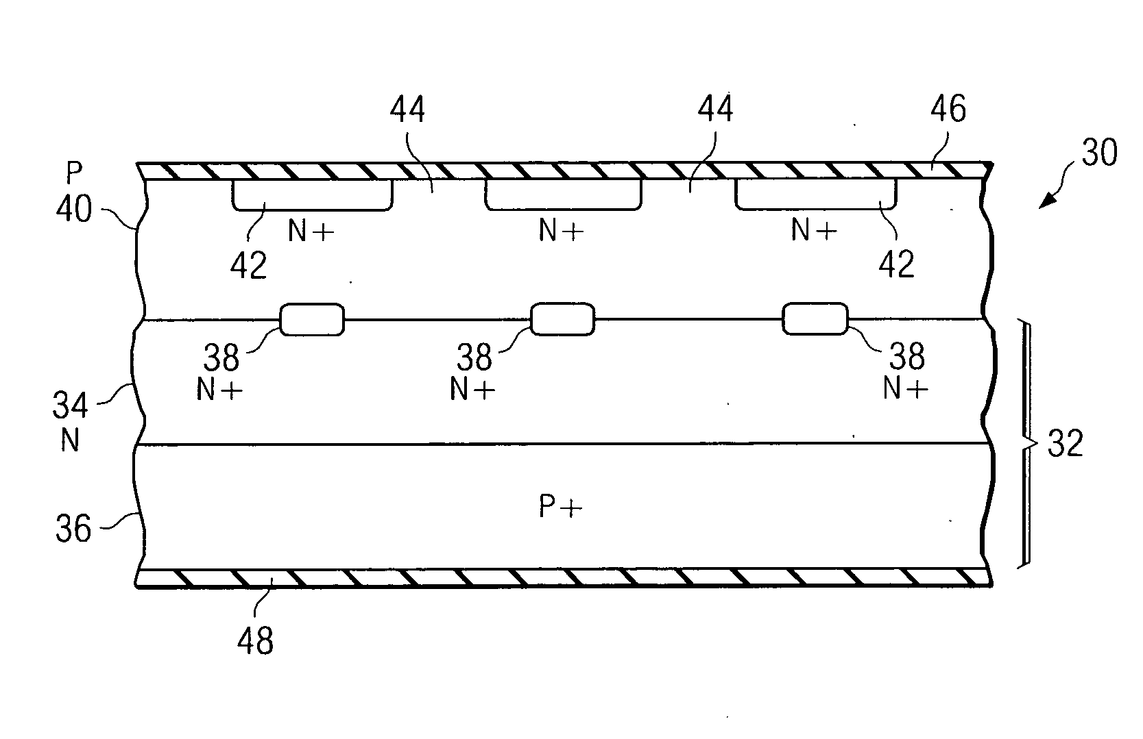
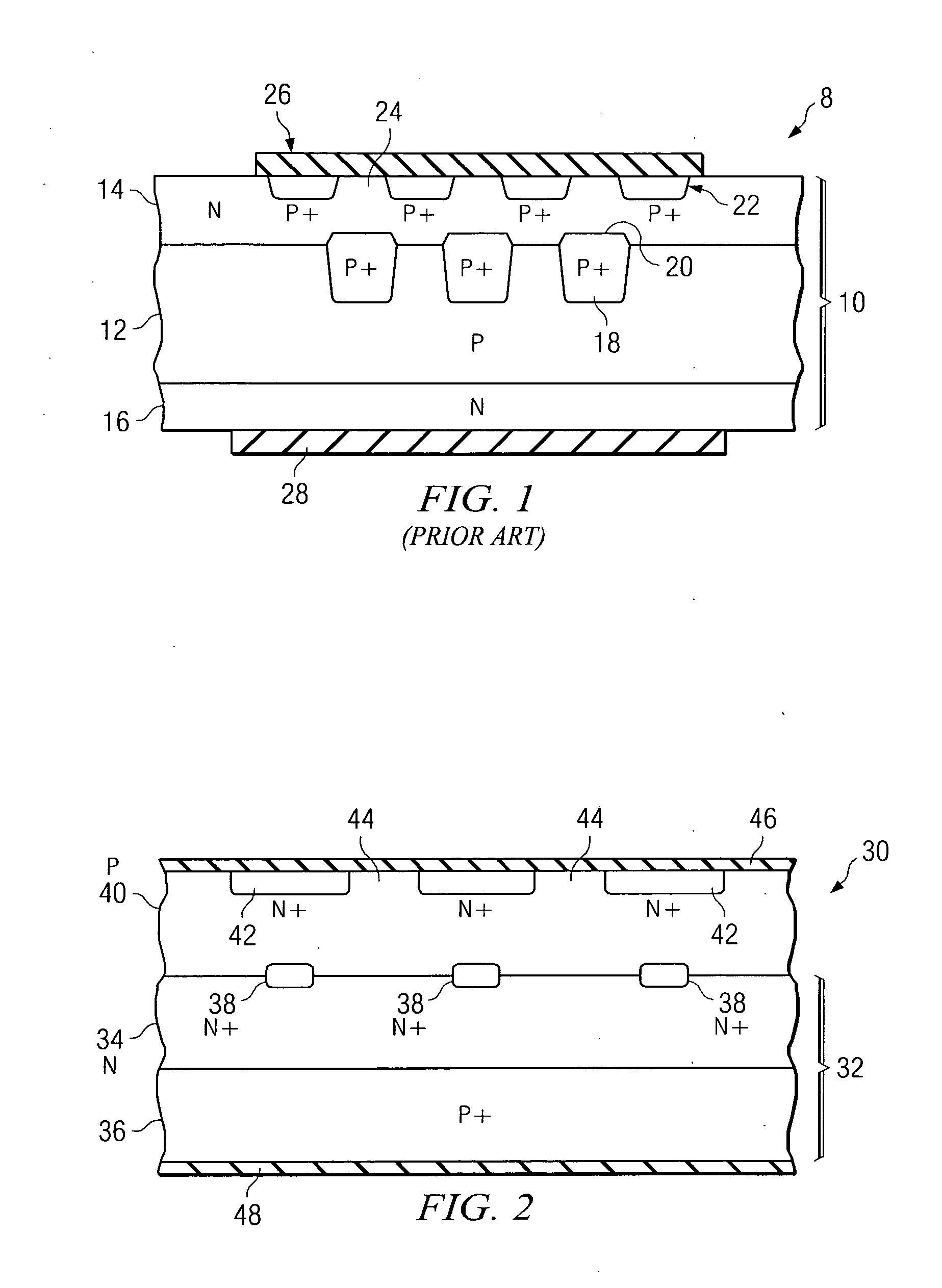
[0044]With reference to FIG. 2, there is illustrated a surge protection device 30 constructed according to one embodiment of the invention. The surge protection devices disclosed herein are four-layer devices that exhibit negative resistance characteristics when full conduction is entered. A starting substrate 32 of a lightly doped N-type impurity is selected. The lightly doped N-type impurity provides a mid-region 34 for the four-layer thyristor 30. The lightly doped mid-region 34 minimizes the capacitance of the chip, it being understood that the depletion region of lightly doped junctions is wide, thus exhibiting a low capacitance as compared to junctions formed between heavily doped regions. The backside of the substrate is then processed to diffuse a P-type impurity therein to form a heavily doped P+ anode region 36.

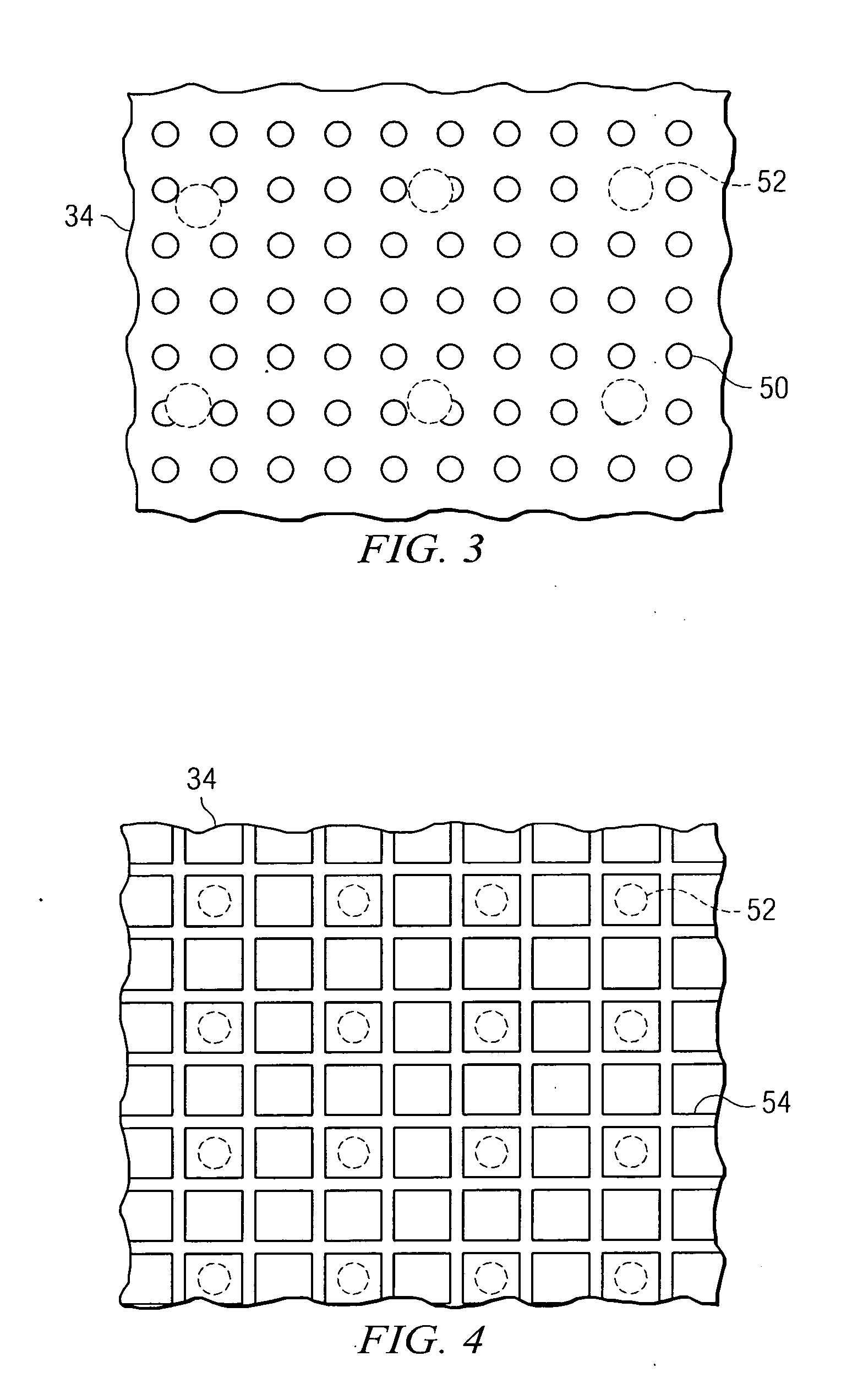
[0045]Next, the wafer is masked with a silicon oxide or nitride mask to define openings for the formation of the buried regions 38. The openings in the mask can be ...


PUM


Abstract

A surge protection device with small-area buried regions (38, 60) to minimize the device capacitance. The doped regions (38, 60) are formed either in a semiconductor substrate (34), or in an epitaxial layer (82), and then an epitaxial layer (40, 84) is formed thereover to bury the doped regions (38, 60). The small features of the buried regions (38, 60) are maintained as such by minimizing high temperature and long duration processing of the chip. An emitter (42, 86) is formed in the epitaxial layer (40, 84).

Description

TECHNICAL FIELD OF THE INVENTION[0001]The present invention relates in general to semiconductor devices, and more particularly to semiconductor surge protection devices.BACKGROUND OF THE INVENTION[0002]Overvoltage protection devices, or surge protection devices, have been highly developed for protecting electrical equipment, especially semiconductor circuits, from damage due to dangerous voltage transients. Voltage transients occurring on conductors, such as communication lines, may be caused by lightning strikes, by electrostatic discharges, electromagnetic fields, etc. Overvoltage protection devices have typically included four layer semiconductor devices, namely thyristors. Ideally, an overvoltage protection device should respond very rapidly to suppress high speed transient voltages with very little overshoot, have a very high current-carrying capability, and exhibit very little capacitance.[0003]One overvoltage protection device that has experienced widespread use is a two-term...

Claims


Application Information

Patent Timeline
IPC IPC(8): H01L29/66H01L21/332
CPCH01L27/0259H01L29/87H01L29/66121
Inventor RODRIGUES, RICHARD A.
Owner LITTELFUSE INC
Why Eureka
Try Eureka