Mos device and process having low resistance silicide interface using additional source/drain implant

a technology of silicide interface and mos, which is applied in the direction of semiconductor devices, electrical devices, transistors, etc., can solve the problems of 45 nm nodes, yield issues, and insufficient improvement to overcome the reduction of doping concentration at state of the art processes, and achieve low resistance, low silicide interface resistance, and low pipe density

Active Publication Date: 2009-03-05
TEXAS INSTR INC
View PDF4 Cites 47 Cited by
  • Summary
  • Abstract
  • Description
  • Claims
  • Application Information

AI Technical Summary

Benefits of technology

[0009]An integrated circuit (IC) includes a semiconductor substrate, a least one MOS transistor formed in or on the substrate, the MOS transistor including a source and drain doped with a first dopant type having a channel region of a second dopant type interposed between, and a gate electrode and a gate insulator over the channel region. A silicide layer forming a low resistance contact is at an interface region at a surface portion of the source and drain. At the interface region a chemical concentration of the first dopant is at least 5×1020 cm−3. Silicide interfaces according to the invention generally provide MOS transistor with low silicide interface resistance, low pipe density, with an acceptably small impact on short channel behavior.

Problems solved by technology

For example, Ni—Pt silicides, instead of Ni, allows increasing the reaction temperature to about 475-500 C. However, while a modest improvement generally results, the improvement is not sufficient to overcome the reduction in doping concentration at state of the art processes, such as at the 45 nm node.
Due to silicide integrity concerns for silicides, including Ni or NiPt silicides, the maximum temperature generally allowed after metal interface layer deposition (e.g. NiPt) is generally less than 500 C, such as about 475 C. Temperatures over about 500 C are known to lead to yield issues mainly due to silicide agglomeration.
While the agglomeration related failures generally do not result in hard failures (i.e. some devices will work), the fraction of failed devices increases substantially as the temperature is increased and the junction depth is decreased, reducing the yield to an unacceptable level for many processes.
Moreover, too high a doping concentration is known to result in an increase in SCE.
The present Inventors have found that maximizing the dopant surface concentration of the source and drain is not necessarily optimal, since the silicide formation process can consume a significant portion of the Si at the surface, such as about 200 A. The energy of the XSD implant(s) are generally selected to provide an as implanted peak from 150 A to 500 A measured from the surface.
A design issue regarding the XSD implant parameters is that the additional dose (above the conventional SD dose) should not result in degraded short channel effects (SCE), since when the deep SD and XSD are performed using the same masking level, the XSD dose generally sees the high temperature deep SD anneal (>950 C), such as a RTA spike anneal which is generally performed at a temperature>1000 C as described below.
However, in the case of boron implant for PMOS, an amorphous region is generally not obtained.
Although increased activation does generally result from the laser anneal including the XSD implanted dopant, this high activation occurs before deactivation due to silicide PA in the contact region, and the increased activation is thus lost due to PA.

Method used


Image

  • Mos device and process having low resistance silicide interface using additional source/drain implant
  • Mos device and process having low resistance silicide interface using additional source/drain implant
  • Mos device and process having low resistance silicide interface using additional source/drain implant

Examples


Embodiment Construction

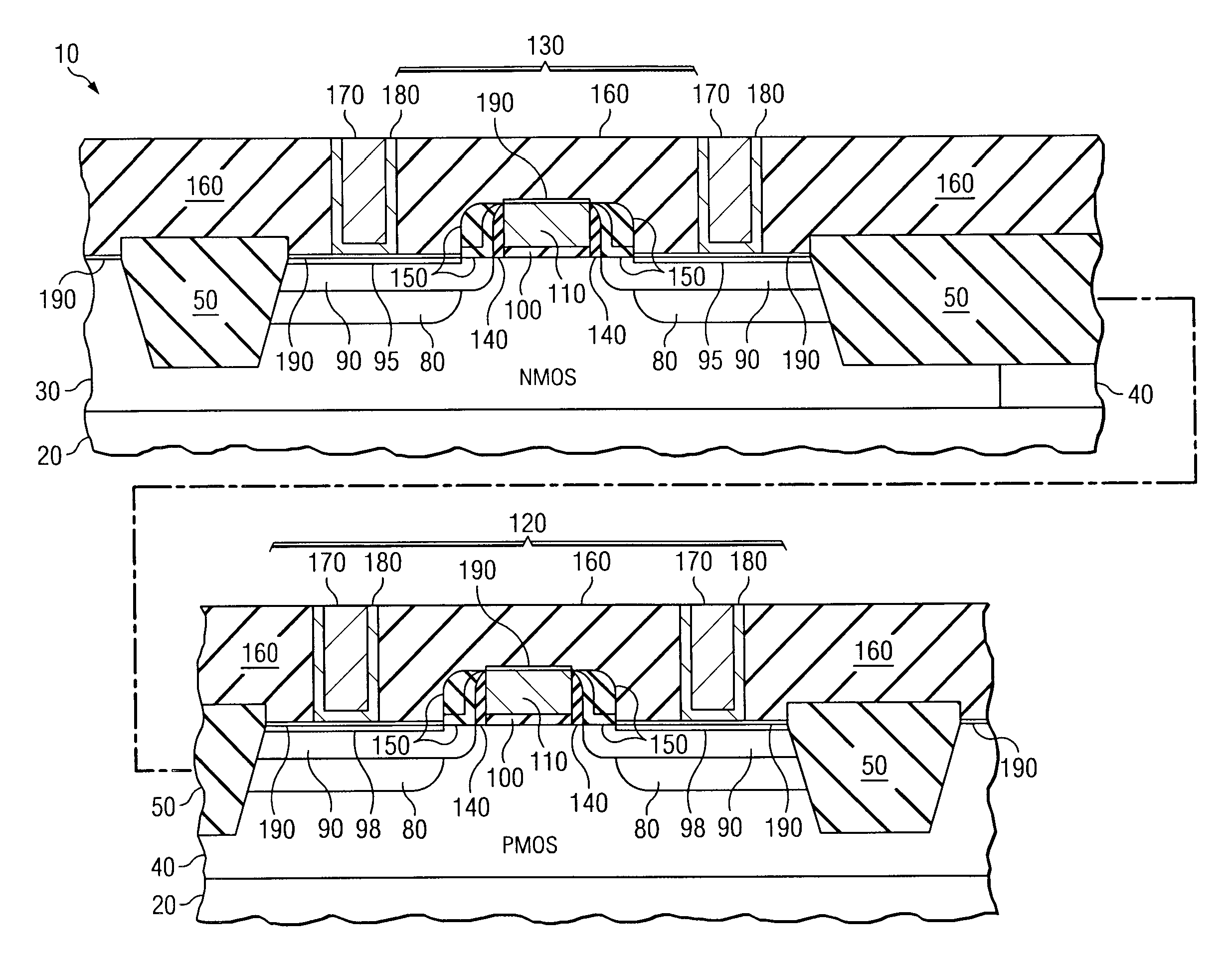
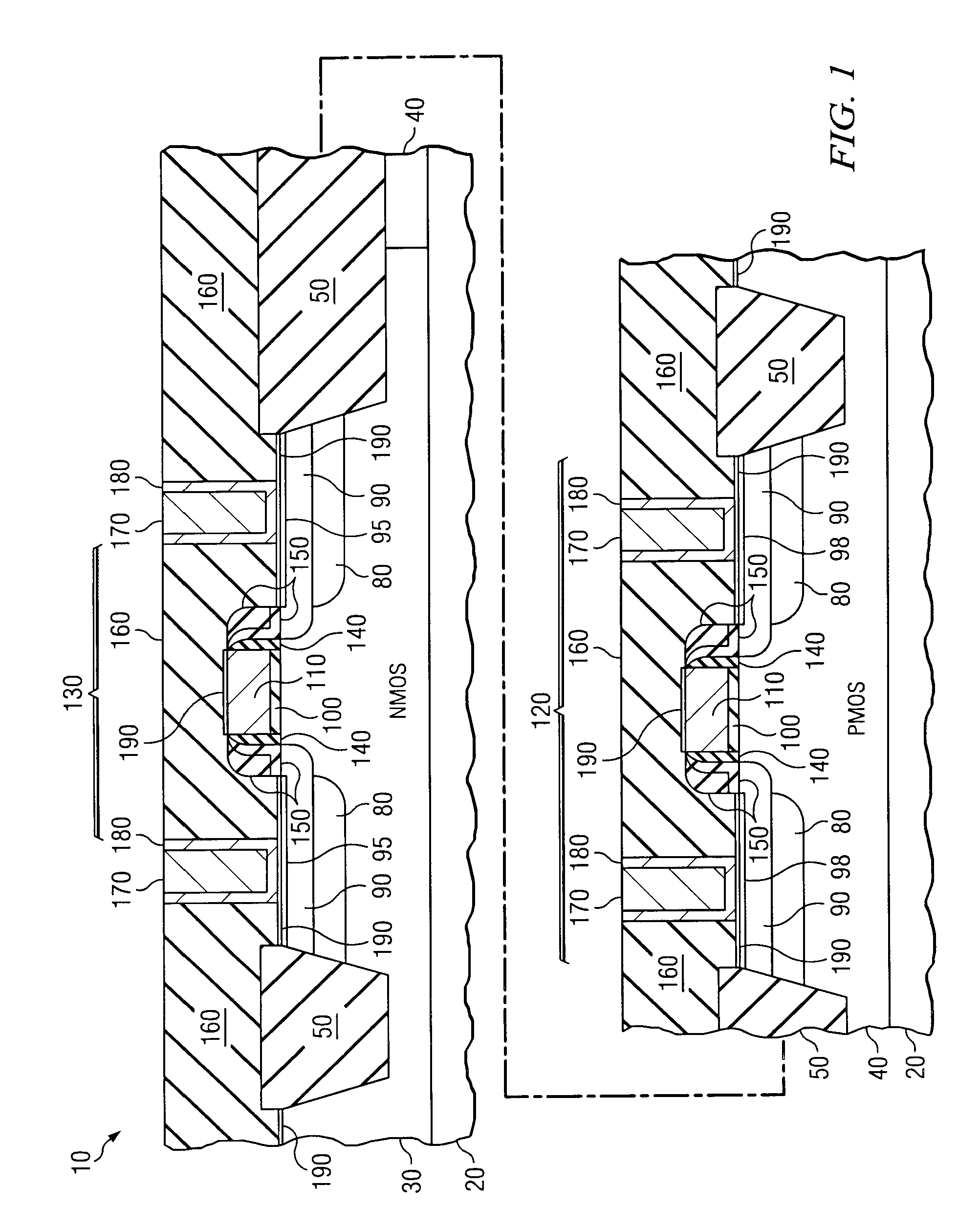
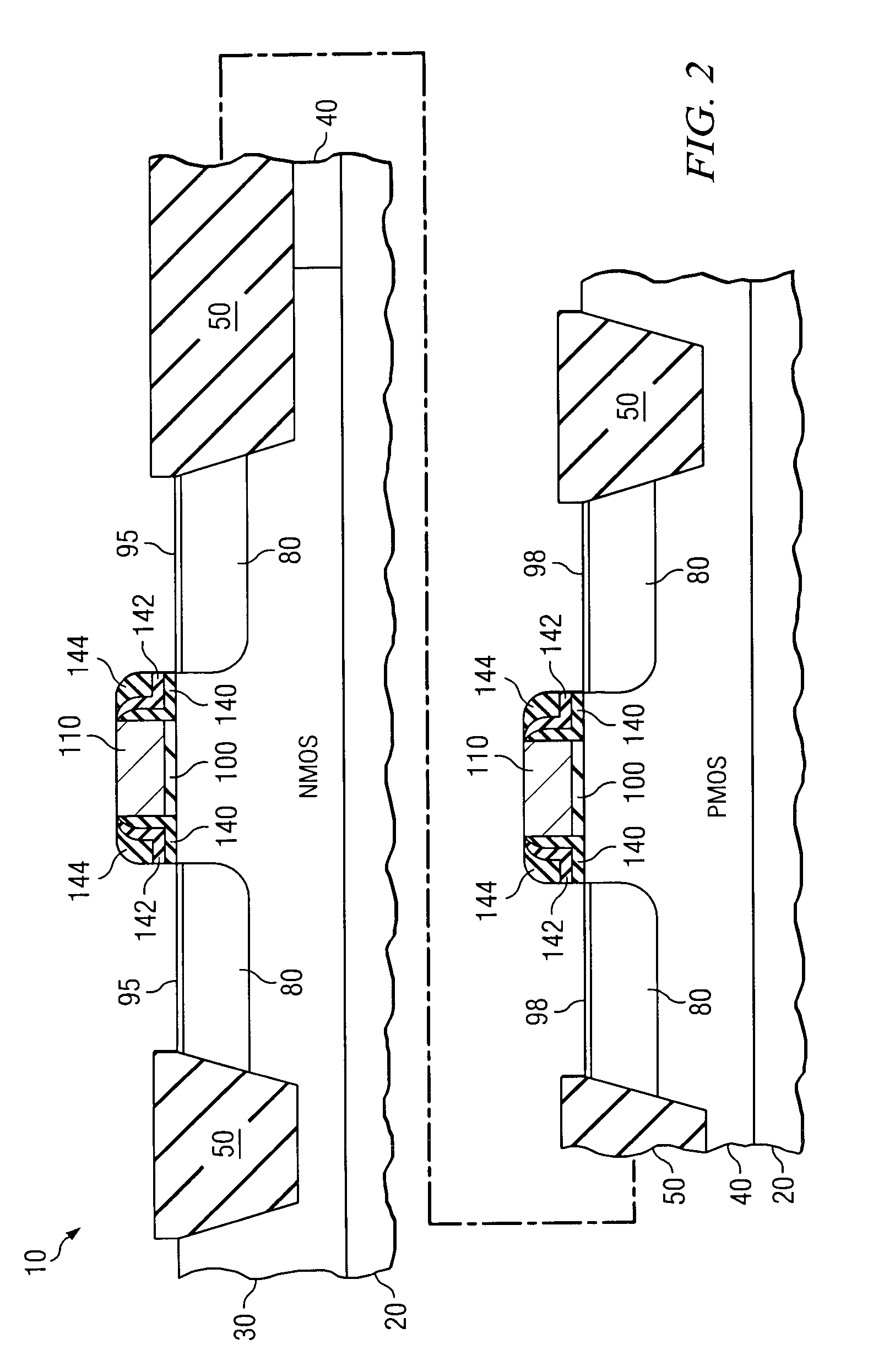
[0019]The present invention is described with reference to the attached figures, wherein like reference numerals are used throughout the figures to designate similar or equivalent elements. The figures are not drawn to scale and they are provided merely to illustrate the instant invention. Several aspects of the invention are described below with reference to example applications for illustration. It should be understood that numerous specific details, relationships, and methods are set forth to provide a full understanding of the invention. One having ordinary skill in the relevant art, however, will readily recognize that the invention can be practiced without one or more of the specific details or with other methods. In other instances, well-known structures or operations are not shown in detail to avoid obscuring the invention. The present invention is not limited by the illustrated ordering of acts or events, as some acts may occur in different orders and / or concurrently with o...


PUM


Abstract

An integrated circuit (IC) includes a semiconductor substrate, a least one MOS transistor formed in or on the substrate, the MOS transistor including a source and drain doped with a first dopant type having a channel region of a second dopant type interposed between, and a gate electrode and a gate insulator over the channel region. A silicide layer forming a low resistance contact is at an interface region at a surface portion of the source and drain. At the interface region a chemical concentration of the first dopant is at least 5×1020 cm−3. Silicide interfaces according to the invention provide MOS transistor with a low silicide interface resistance, low pipe density, with an acceptably small impact on short channel behavior.

Description

FIELD OF THE INVENTION[0001]The present invention relates to complementary metal oxide semiconductor (CMOS) device manufacturing and resulting CMOS devices, and in particular to a method of fabricating a shallow junction CMOS device in which the silicide interface resistance is low, while still limiting both yield reducing pipes and the short channel effect (SCE).BACKGROUND[0002]Advances in the miniaturization of complementary-metal-oxide-semiconductor (CMOS) devices have been a key driving force behind the explosive growth of various network centric computing products such as ASIC high-speed microprocessors and memories, low power hand-held computing devices and advanced multi-media audio and video devices. Smaller CMOS devices typically equate to faster switching times which in turn lead to faster and better performing end user systems.[0003]It is well known that as the contact area decreases, contact resistance increases, and as the active semiconductor dopant level at the contac...

Claims


Application Information

Patent Timeline
Patent Type & Authority Applications(United States)
IPC IPC(8): H01L21/8238H01L29/94
CPCH01L21/26513H01L21/823814H01L29/7833H01L29/6656H01L29/6659H01L29/665
Inventor OBRADOVIC, BORNAEKBOTE, SHASHANKVISOKAY, MARK
Owner TEXAS INSTR INC
Why Eureka
Try Eureka