Anisotropic film and method of manufacturing anisotropic film

a technology of anisotropic film and anisotropic film, which is applied in the direction of elastomeric connecting element apparatus, instruments, and semiconductor/solid-state device details, etc., can solve the problems of difficult fabrication of structures in which at least a portion of structures has dimensions at the nanometer level, nanometers, and low etching resistance of patterns, etc., to achieve excellent anisotropy and superior workability and handling properties

Inactive Publication Date: 2009-03-05
TOKYO OHKA KOGYO CO LTD +1
View PDF12 Cites 24 Cited by
  • Summary
  • Abstract
  • Description
  • Claims
  • Application Information

AI Technical Summary

Benefits of technology

[0027]According to the present invention, an anisotropic film can be provided that exhibits excellent anisotropy, as well as superior workability and handling properties.

Problems solved by technology

However, using the methods proposed to date, fabricating a structure in which at least a portion of the structure has dimensions at the nanometer level (namely, a nanostructure), such as a structure composed of a metal layer having a thickness within a range from several nanometers to several tens of nanometers, has proven very difficult.
For example, using a method (1) described above, not only is the actual formation of a nanosize pattern extremely difficult, but even if such a nanosize pattern were to be formed, the etching resistance of the pattern is low and the etching selectivity ratio relative to the metal substrate is poor, meaning obtaining a satisfactory nanostructure is problematic.
Furthermore, a method (2) described above suffers from a similar problem to the method (1) in that actual formation of the microscopic pattern is extremely difficult, and moreover, conducting a plating treatment within such a microscopic pattern is also difficult.
Formation of a structure with a large aspect ratio (the ratio of height relative to width) such as a line-shaped or columnar structure is particularly difficult.

Method used


Image

  • Anisotropic film and method of manufacturing anisotropic film
  • Anisotropic film and method of manufacturing anisotropic film
  • Anisotropic film and method of manufacturing anisotropic film

Examples


first embodiment

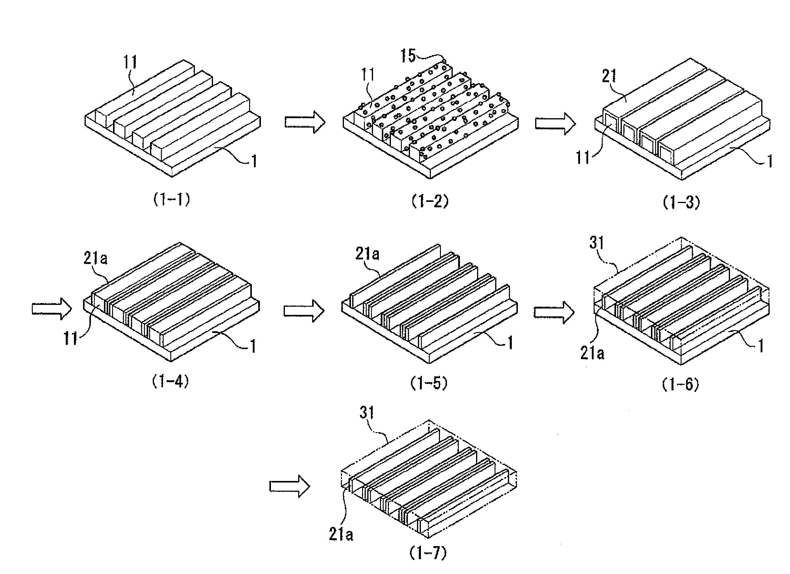
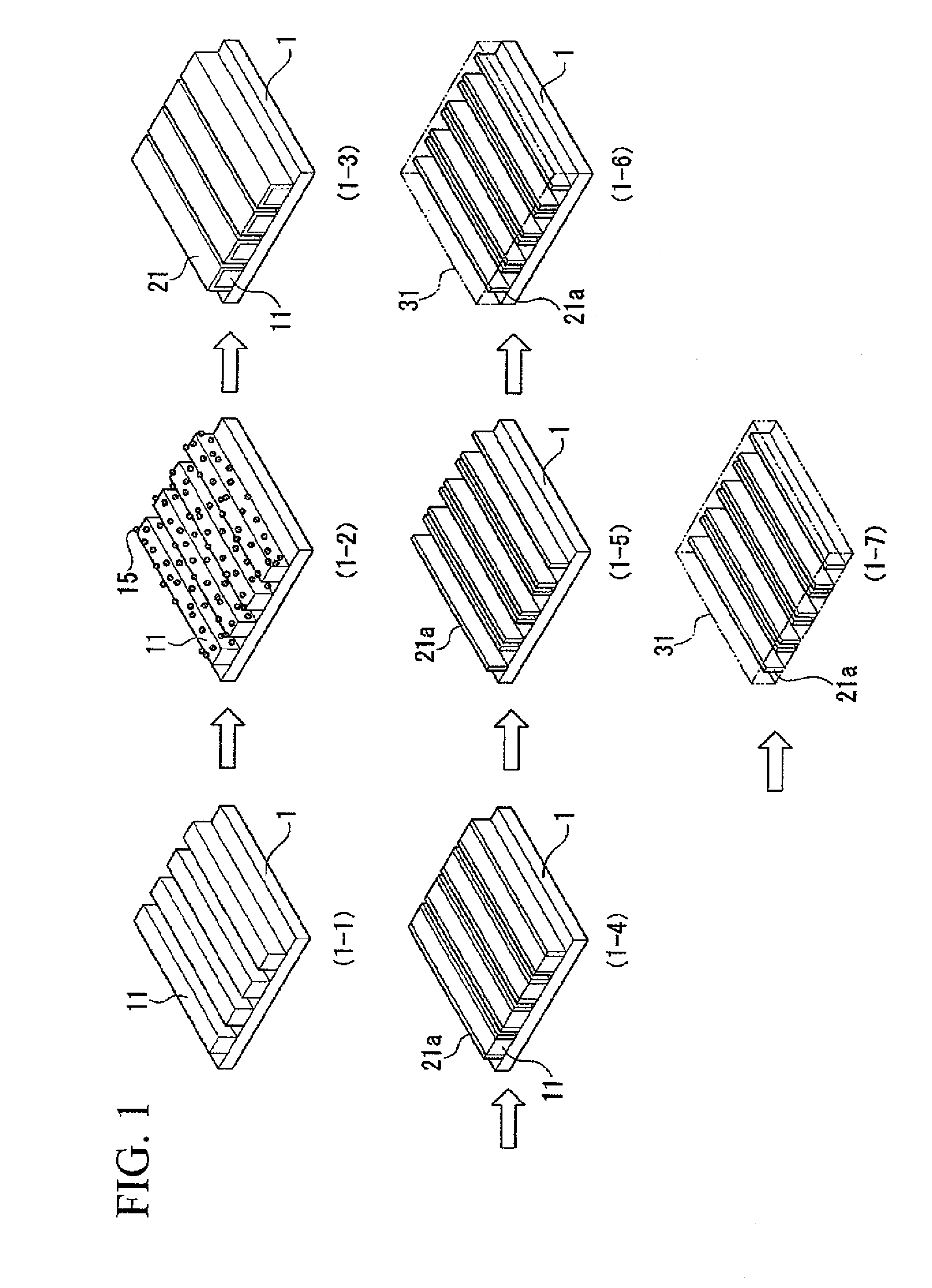
[0317]FIG. 1 shows a flowchart for a first embodiment.

[0318]In this embodiment, first, a template 11 composed of a rectangular line structure is formed on a substrate 1 (1-1).

[0319]Next, a catalyst (fine metal particles) 15 is introduced onto the surface of the template 11 (1-2). Electroless plating is then performed on the surface of the template 11, thereby forming a coating film 21 composed of a metal layer (1-3). Next, the top portion of the coating film 21 is removed along a plane parallel to the substrate 1, thereby exposing the template 11 (1-4). At this point, a portion of the template 11 may also be removed together with the top portion of the coating film 21. Finally, the template 11 is removed. As a result, only the side wall portions 21a of the coating film 21 remain on the substrate 1 (1-5).

[0320]Subsequently, a resin film 31 is formed on the substrate 1 having the side wall portions 21a formed thereon (1-6). This resin film 31 is then detached from the substrate 1 with...

example 1

Production of Anisotropic Film Containing Line-Shaped Gold Nanostructures Arranged in Parallel

[0351]First, a silicon wafer substrate having an organic resist (product name: TDUR-P015 PM, manufactured by Tokyo Ohka Kogyo Co., Ltd.) in which rectangular line-shaped structures having a width of approximately 400 nm and a height of approximately 700 nm had been formed by a lithography process was subjected to an oxygen plasma treatment (power: 10 W, pressure: 24 Pa, treatment time: 3 minutes), thereby reducing the size of the template to a width of approximately 200 nm and a height of approximately 350 nm, while also activating the surface of the template.

[0352]Subsequently, the substrate was dipped for two minutes in 20 ml of an aqueous solution of tin chloride (0.022 M), washed twice with deionized water, and then dried under a stream of nitrogen gas. The substrate was then dipped for 5 minutes in 20 ml of an aqueous solution of palladium chloride (0.0015 M), washed twice with deioniz...

example 2

Production of Anisotropic Film Containing Line-Shaped Gold Nanostructures Arranged in Parallel

[0358]First, a silicon wafer substrate having an organic resist (product name: TCIR-ZR9000 PB, manufactured by Tokyo Ohka Kogyo Co., Ltd.) in which rectangular line-shaped structures having a width of approximately 5 μm and a height of approximately 500 nm had been formed by a lithography process was subjected to an oxygen plasma treatment (power: 10 W, pressure: 24 Pa, treatment time: 3 seconds), thereby activating the surface of the template.

[0359]Subsequently, the substrate was dipped for two minutes in 20 ml of an aqueous solution of tin chloride (0.022 M), washed twice with deionized water, and then dried under a stream of nitrogen gas. The substrate was then dipped for 5 minutes in 20 ml of an aqueous solution of palladium chloride (0.0015 M), washed twice with deionized water, and then dried under a stream of nitrogen gas. This series of operations was conducted once. Subsequently, 1...


PUM

PropertyMeasurementUnit
diameteraaaaaaaaaa
widthaaaaaaaaaa
widthaaaaaaaaaa

Abstract

An anisotropic film is disclosed in which a line-shaped nanostructure is disposed inside a resin film. Also disclosed is a method of producing an anisotropic film that includes: forming a metal nanostructure on a substrate, forming a resin film that embeds the metal nanostructure, and detaching the resin film from the substrate, wherein the step of forming the metal nanostructure on the substrate includes: at least, forming a coating film on the surface of a template provided on the substrate, the coating film including a metal layer formed by electroless plating; and removing a portion or all of the template while retaining a portion or all of the coating film, or removing a portion of the coating film. Also disclosed is an anisotropic film produced using the method of producing an anisotropic film.

Description

TECHNICAL FIELD[0001]The present invention relates to an anisotropic film having a nanostructure within a resin film, and a method of producing an anisotropic film having a nanostructure that includes at least a metal layer.[0002]This application claims priority from Japanese Patent Application No. 2007-227934 filed on Sep. 3, 2007, the disclosure of which is incorporated by reference herein.BACKGROUND ART[0003]In recent years, techniques for fabricating microscopic structures have begun to show considerable promise for application in all manner of fields. In particular, structural bodies that include structures of nanometer size (so-called nanomaterials) exhibit different physical and chemical properties from their corresponding bulk materials, and are therefore attracting enormous interest, both from the fundamental research perspective and the applied research perspective. For example, nanomaterials having a hollow three dimensional structure such as a cylindrical shape are expec...

Claims


Application Information

Patent Timeline
Patent Type & Authority Applications(United States)
IPC IPC(8): B32B3/10B05D5/00B05D3/00B05D3/10H05H1/24
CPCH01L23/4985H01R43/007H05K3/4038H05K2201/10378Y10T428/24802H01L2924/0002H05K2203/0338H01L2924/00
Inventor FUJIKAWA, SHIGENORIKUBO, WAKANAKUNITAKE, TOYOKIHADA, HIDEOFURUYA, SANAE
Owner TOKYO OHKA KOGYO CO LTD
Why Eureka
Try Eureka