Solar cell manufactured using amorphous and nanocrystalline silicon composite thin film, and process for manufacturing the same

a technology of amorphous and nanocrystalline silicon and composite thin films, which is applied in the field of solar cells, can solve the problems of reducing production yield, reducing current generation, and reducing the conversion efficiency of solar cells, so as to achieve excellent conversion efficiency to a solar cell, improve photoelectric conversion efficiency, and reduce production cost

Inactive Publication Date: 2009-03-19
LG ELECTRONICS INC
View PDF4 Cites 29 Cited by
  • Summary
  • Abstract
  • Description
  • Claims
  • Application Information

AI Technical Summary

Benefits of technology

[0015]Another object of the present invention is to provide a solar cell with enhanced photoelectric conversion efficiency and reduced defects, manufactured by fabricating a composite thin film with amorphous silicon and crystalline silicon which are usually used in conventional solar cells.
[0056]According to the present invention, the composition for the composite thin film contained in the solar cell is provided, which comprises the amorphous silicon precursor and the nanocrystalline silicon. Using the composition can allow manufacture of the solar cell having the composite thin film with high efficiencies by adopting simple and convenient processes and low price economical equipment, so that the present invention has an economic advantage in view of the production cost.

Problems solved by technology

However, a solar cell with a lamination structure comprising multiple silicon layers with different particle phases, has a few problems such as complicated and longer processes, restriction of current generated from light by one of the solar cell layers having the least current, due to the structure of the solar cell being in a series connection form, etc.
Therefore, the above solar cell has a difficulty in accomplishing the higher conversion efficiency unless photoelectric currents generated from the solar cell layers are designed to be identical.
However, the formation of silicon film using CVD normally adopts a gas-phase reaction and, in turn, the reaction is carried out on walls of a reaction chamber or in a gas phase thereby generating contaminants or impurities which lead to decrease in production yield.
Furthermore, the CVD has a low reaction velocity thereby further reducing productivity.
The CVD also includes a drawback of requiring complicated and expensive installations because it uses specific apparatuses such as vacuum equipment and a high frequency generator.
For raw materials used in the CVD, gaseous silane with high toxicity and reactivity is used, which is difficult to be managed and / or handled and needs more expensive equipment for management or maintenance thereof.
Meanwhile, carrier lifetime of the solar cell which plays an important role in the conversion efficiency of the solar cell is affected by defects existing in the composite thin film.
The defects promote recombination of the carrier and reduce the carrier lifetime, thereby decreasing the conversion efficiency of the solar cell.

Method used


Image

  • Solar cell manufactured using amorphous and nanocrystalline silicon composite thin film, and process for manufacturing the same
  • Solar cell manufactured using amorphous and nanocrystalline silicon composite thin film, and process for manufacturing the same
  • Solar cell manufactured using amorphous and nanocrystalline silicon composite thin film, and process for manufacturing the same

Examples


Embodiment Construction

[0062]Hereafter, the present invention will be described in detail in the following example with reference to the accompanying drawings.

[0063]General constructions and functions commonly known in related arts are not essential components for the present invention and have not been described in detail herein, in order to avoid unnecessary duplication of explanation thereof.

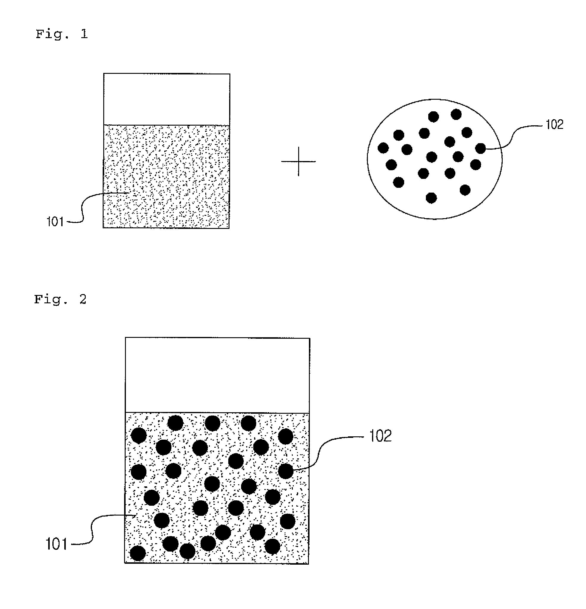
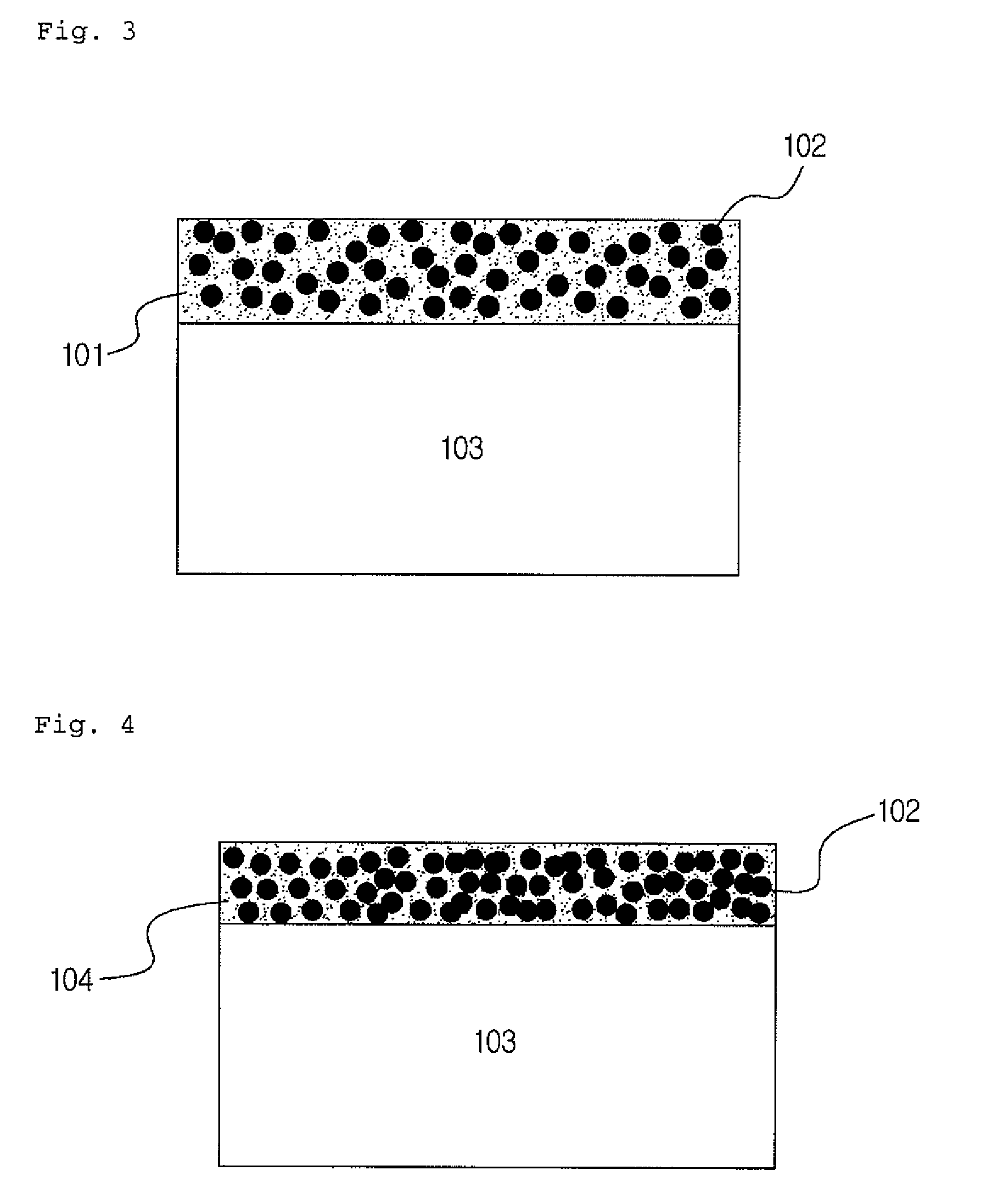
[0064]FIGS. 1 and 2 illustrate a process of preparing a mixture of the silicon precursor and the crystalline silicon nanoparticles according to one embodiment of the present invention.

[0065]The silicon precursor may be a liquid silane SiH4 composition 101.

[0066]The liquid silane composition can optionally include an organic solvent.

[0067]The silane composition 101 may include a colloidal silicon dispersed in an appropriate dispersing solvent. Such colloidal silicon is used for increasing silicon concentration of the silane composition 101 and can regulate thickness of a coating film by silicon content of in the com...


PUM

PropertyMeasurementUnit
sizeaaaaaaaaaa
particle sizeaaaaaaaaaa
temperatureaaaaaaaaaa

Abstract

Disclosed are a solar cell manufactured using a composite thin film comprising amorphous silicon and nanocrystalline silicon, a method of manufacturing the solar cell, and a composition for the composite thin film used in manufacturing the solar cell. More particularly, a silicon semiconductor layer in the solar cell is fabricated by using the composite thin film comprising the amorphous silicon and the nanocrystalline silicon, the composite thin film being formed by dispersing nanoparticles of the crystalline silicon in a liquid silicon precursor and modifying them.The solar cell of the present invention is manufactured by dispersing the crystalline silicon nanoparticles in the liquid silicon precursor, coating the dispersion on a substrate or printing the substrate with the dispersion, and heating the coated or printed substrate to modify the liquid silicon precursor into the amorphous silicon.According to the present invention, any expensive equipment requiring alternative complicated installations is not needed to form a composite thin film comprising both of amorphous silicon and crystalline silicon. In addition, it is possible to form a composite thin film comprising plural materials with different band gap energy which can remarkably improve conversion efficiency of a solar cell by using a liquid precursor and nanocrystalline particles in a solution process with low production cost.

Description

[0001]This application claims priority to Korean Patent Application No. 10-2007-0094787, filed on Sep. 18, 2007, in the Korean Intellectual Property Office, the entire contents of which are hereby incorporated by reference.BACKGROUND OF THE INVENTION[0002]1. Field of the Invention[0003]The present invention relates to solar cells manufactured by using amorphous silicon and nanocrystalline silicon based composite thin films and manufacturing processes thereof, more particularly, to a method of manufacturing solar cells with silicon semiconductor films formed of composite thin films comprising amorphous silicon and nanocrystalline silicon, each of the composite thin films being formed with low production cost using a silicon precursor and silicon nanoparticles.[0004]2. Description of the Related Art[0005]Increase in conversion efficiency is very important in solar cell fields. Using together two or more of materials having different optical band-gaps can improve application efficiency...

Claims


Application Information

Patent Timeline
Patent Type & Authority Applications(United States)
IPC IPC(8): H01L31/00H01L31/04H01L31/075H01L31/18
CPCB82Y20/00B82Y30/00H01L31/035281Y02E10/548H01L31/03845H01L31/075H01L31/202H01L31/03762H01L21/228Y02P70/50H01L31/0216H01L31/18H01L31/0445
Inventor CHOI, YONG WOOCHOE, YOUNG HOKIM, HYUNG SEOKLEE, YOUNG HEE
Owner LG ELECTRONICS INC
Why Eureka
Try Eureka