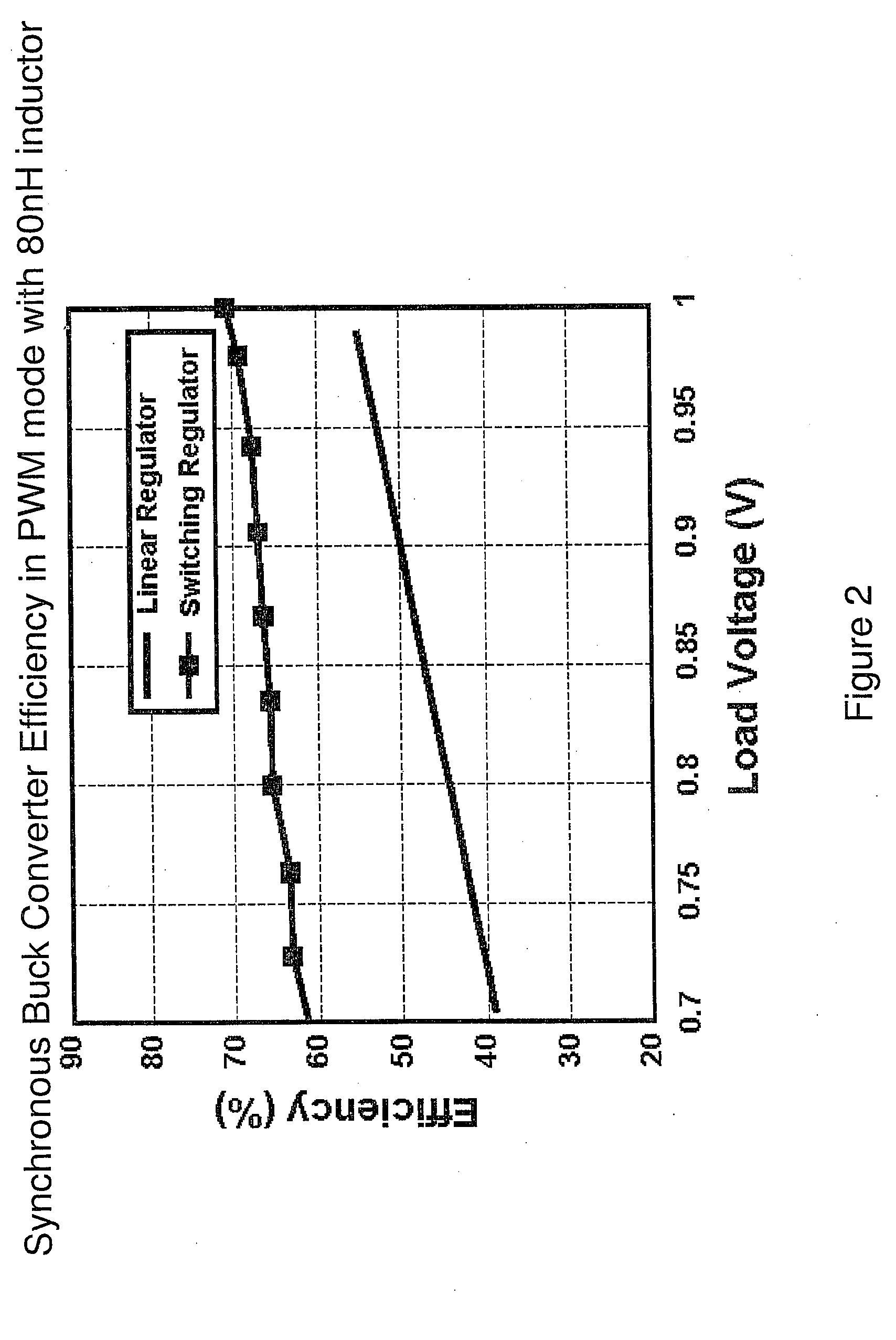
In applications where the output voltage of the LDO is low, for example, less than 1V with a 1.8V input supply, the efficiency may be quite low, which means an increase in wasted power.
This inefficiency leads to shorter battery life, or shorter battery
operating time between charges for rechargeable devices, for example.
Present circuits may often operate at even lower operating voltages and this inefficiency becomes more problematic as operating voltages for integrated circuits decrease.
As integration increases and the size of the devices is reduced, the use of off-
chip regulators, and / or of off-
chip components, becomes undesirable for several reasons.
Further, the use of switching regulators with typical switching frequencies in
wireless or cellular device applications can create tone frequencies and
noise problems that are unacceptable.
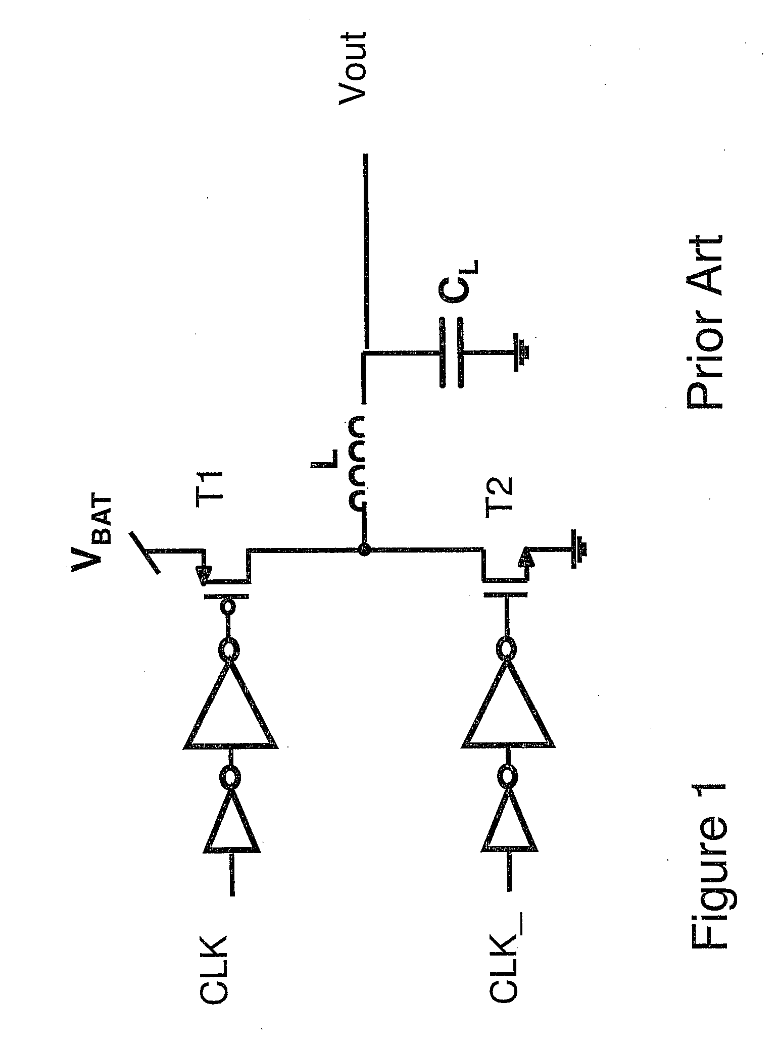
However, the switching of the power device results in a regulated average output voltage with voltage ripples around the regulated level.
This circuit, however, has two significant problems that make it impractical for use as a
regulator.
First, the reduction in the
inductor value results in a larger current
ripple in the inductor, and thus a larger output voltage
ripple.
Second, a significant efficiency loss is observed due to operating the inductor in
discontinuous conduction mode, which is a direct unavoidable result of reducing the inductor value while at the same time maintaining the fixed
switching frequency and the PWM control scheme.
However the use of a PFM control scheme is not practical for many applications because the varying frequency of the switching circuitry produces an unpredictable
ripple voltage spectrum at the output that is a function of the load current, and thus cannot be easily filtered.
In
wireless applications in particular, or in other
noise-sensitive applications, using a PFM control scheme is highly undesirable due to its unpredictability.
However, the use of PFM control schemes creates tones or spurs in the output voltage Vout that are not predictable, making effective filtering of these tones impracticable.
Thus, the use of this kind of control to achieve
voltage regulation in a switched capacitor DC-
DC converter is not preferable for many applications where the unpredictable
tone frequency is not acceptable, for example, in certain analog,
wireless, cellular or other transmitting and receiving technologies where the tone
noise would make operation of the circuitry coupled to the output voltage Vout in the load impossible.
While these approaches will not have the same tone or noise unpredictability problems of the PFM control scheme, other problems arise.
However, the loss mechanisms associated with switched capacitor circuits do not scale with the load power in these schemes.
Also, effective output regulation in response to wide variations in load power cannot be obtained using switched capacitor DC
converters regulated with these approaches.

