Semiconductor device

a technology of semiconductor devices and semiconductors, applied in semiconductor devices, semiconductor/solid-state device details, electrical apparatus, etc., can solve the problems of unbalanced area occupied by n-channel transistors and an area occupied by p-channel transistors, prevented devices from being highly integrated, and unnecessary space for circuit arrangement, etc., to achieve reduced mobility between n-channel field-effect transistors and p-channel field-effect transistors, the effect of reducing power consumption and reducing

Active Publication Date: 2009-03-26
SEMICON ENERGY LAB CO LTD
View PDF21 Cites 245 Cited by
  • Summary
  • Abstract
  • Description
  • Claims
  • Application Information

AI Technical Summary

Benefits of technology

[0023]In n-channel and p-channel semiconductor layers, it is preferable that a plane orientation of a surface which is parallel to an insulating surface be {110} and a crystal axis in a channel length direction be <110>. This is because difference in mobility between the n-channel field-effect transistor and the p-channel field-effect transistor can be reduced.
[0024...

Problems solved by technology

Therefore, an area occupied by the n-channel transistor and an area occupied by the p-channel transistor become unbalanced.
As a re...

Method used


Image

  • Semiconductor device
  • Semiconductor device
  • Semiconductor device

Examples


embodiment mode 1

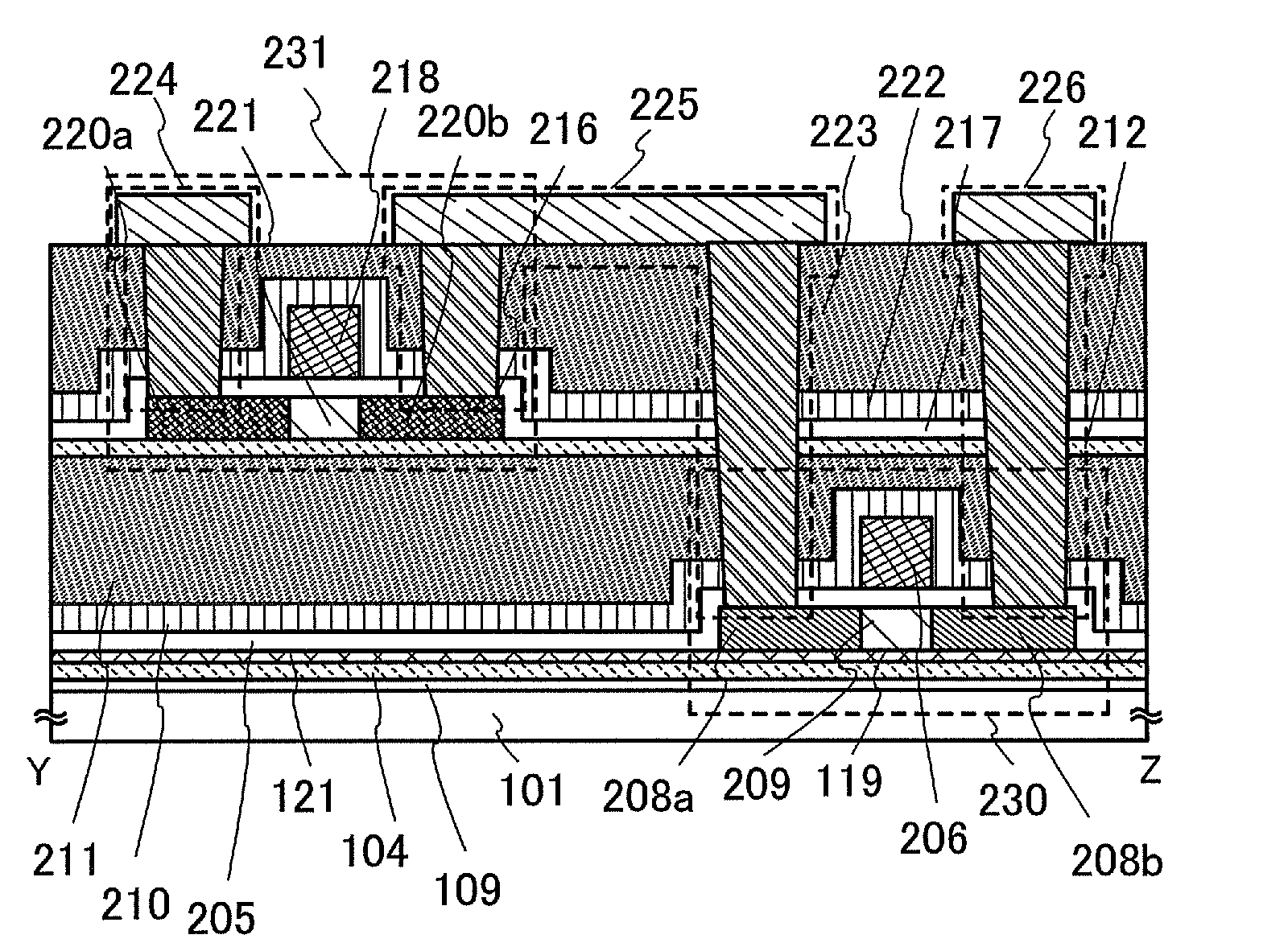
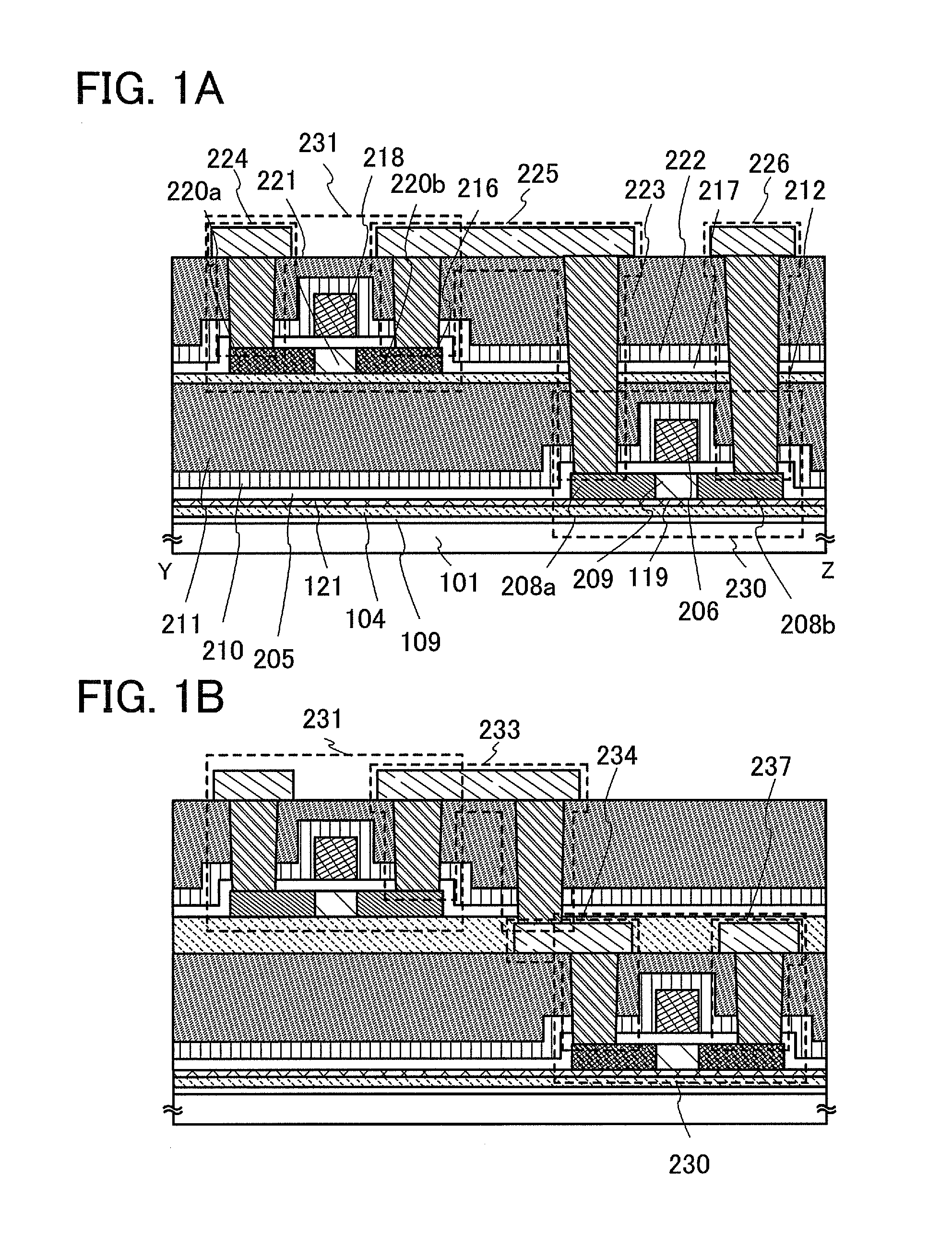
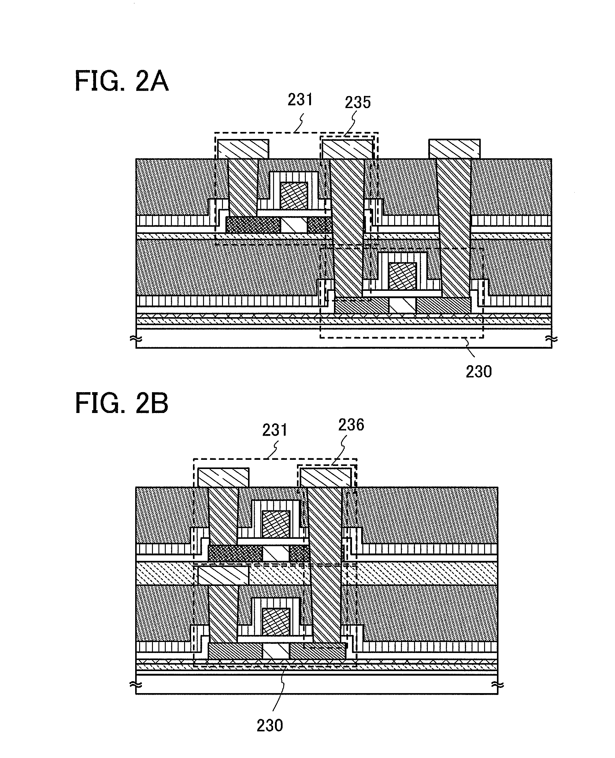
[0050]A method for manufacturing a semiconductor device of the present invention is described with reference to FIGS. 1A and 1B, FIGS. 2A and 2B, FIGS. 3A to 3D, and FIGS. 4A to 4D. This embodiment mode describes a complementary metal oxide semiconductor (CMOS) as an example of semiconductor devices which include more highly integrated and higher performance semiconductor elements.

[0051]In this embodiment mode, semiconductor elements having a semiconductor layer which is separated from a semiconductor substrate and is bonded to a supporting substrate having an insulating surface are stacked with an insulating layer interposed therebetween. The semiconductor element which is to be stacked includes a semiconductor element having a semiconductor layer in which a distortion is caused to a channel formation region by an insulating film. A single-crystal semiconductor substrate is preferably used as the semiconductor substrate, and a single-crystal semiconductor layer is preferably formed...

embodiment mode 2

[0179]This embodiment mode describes an example of a step for bonding a semiconductor layer from a semiconductor substrate to a supporting substrate, which is different from that in Embodiment Mode 1. Therefore, repetitive descriptions for the same components as or components having similar functions to the components in Embodiment Mode 1 are omitted.

[0180]In this embodiment mode, when a semiconductor layer is transferred from a semiconductor substrate, the semiconductor substrate is selectively etched (this step is also referred to as a groove processing), and a plurality of semiconductor layers which are divided to have the size of semiconductor elements to be manufactured are transferred to a supporting substrate. Thus, a plurality of island-shaped semiconductor layers can be formed over the supporting substrate. The semiconductor layers which are processed into an element size in advance are transferred; therefore, the semiconductor layers can be transferred to the supporting su...

embodiment mode 3

[0199]This embodiment mode describes an example of a step for bonding a semiconductor layer from a semiconductor substrate to a supporting substrate, which is different from that in Embodiment Mode 1. Therefore, repetitive descriptions for the same components as or components having similar functions to the components in Embodiment Mode 1 are omitted.

[0200]This embodiment mode describes an example in which after a semiconductor layer is separated from a semiconductor substrate, the semiconductor layer is bonded to a supporting substrate.

[0201]As described in Embodiment Mode 2 with reference to FIGS. 5A to 5E, the fragile layer is formed in the semiconductor substrate, and a groove is formed. The groove processing is performed in consideration of the shape of a semiconductor layer of a semiconductor element. That is, in order to transfer the semiconductor layer of the semiconductor element to the supporting substrate, the groove processing is performed on a semiconductor substrate 30...


PUM


Abstract

An object is to realize high performance and low power consumption in a semiconductor device having an SOI structure. In addition, another object is to provide a semiconductor device having a high performance semiconductor element which is more highly integrated. A semiconductor device is such that a plurality of n-channel field-effect transistors and p-channel field-effect transistors are stacked with an interlayer insulating layer interposed therebetween over a substrate having an insulating surface. By controlling a distortion caused to a semiconductor layer due to an insulating film having a stress, a plane orientation of the semiconductor layer, and a crystal axis in a channel length direction, difference in mobility between the n-channel field-effect transistor and the p-channel field-effect transistor can be reduced, whereby current driving capabilities and response speeds of the n-channel field-effect transistor and the p-channel field-effect can be comparable.

Description

BACKGROUND OF THE INVENTION[0001]1. Field of the Invention[0002]The present invention relates to semiconductor devices having a so-called SOI (silicon on insulator) structure in which a semiconductor layer is provided on an insulating surface.[0003]2. Description of the Related Art[0004]As an alternative to an integrated circuit using a silicon wafer which is manufactured by thinly slicing a single-crystal semiconductor ingot, an integrated circuit using a semiconductor substrate which is referred to as a silicon on insulator (hereinafter also referred to as “SOI”) in which a thin single-crystal semiconductor layer is provided on an insulating surface has been developed. The integrated circuit using an SOI substrate has attracted attention as a semiconductor integrated circuit which reduces parasitic capacitance between a transistor and the substrate and improves the performance of a semiconductor integrated circuit.[0005]As a method for manufacturing SOI substrates, a hydrogen ion ...

Claims


Application Information

Patent Timeline
IPC IPC(8): H01L27/08
CPCH01L21/823807H01L21/823871H01L2924/16195H01L23/433H01L23/481H01L23/552H01L27/0688H01L27/1214H01L27/1266H01L29/7843H01L2224/16H01L2224/73253H01L2924/01046H01L2924/01077H01L2924/01078H01L2924/01079H01L2924/09701H01L2924/12044H01L2924/16152H01L27/1229H01L21/31H01L21/8238
Inventor YAMAZAKI, SHUNPEIISOBE, ATSUOGODO, HIROMICHIOKAZAKI, YUTAKA
Owner SEMICON ENERGY LAB CO LTD
Why Eureka
Try Eureka