Profile Engineered Thin Film Devices and Structures

a technology of thin film and engineered components, applied in thermoelectric devices, coatings, liquid/solution decomposition chemical coatings, etc., can solve the problems of premature dielectric breakdown and leakage current, enhanced electric field effect and/or leakage current, and achieve high performance

Active Publication Date: 2009-04-02
ENSURGE MICROPOWER ASA
View PDF32 Cites 85 Cited by
  • Summary
  • Abstract
  • Description
  • Claims
  • Application Information

AI Technical Summary

Benefits of technology

[0007]The present invention concerns devices that include relatively high performance devices containing one or more printed semiconductor (e.g., silicon), insulator (e.g., silicon dioxide) and conductor (e.g., metal) features and processes for manufacturing such features. More specifically, embodiments of the present invention relate to improved processes for making such devices using printed (e.g., inkjet pr...

Problems solved by technology

This can lead to enhanced electric field effects and/or leakage current at a given operating voltage at these locations.
Specifically, thin portions of a therm...

Method used


Image

  • Profile Engineered Thin Film Devices and Structures
  • Profile Engineered Thin Film Devices and Structures
  • Profile Engineered Thin Film Devices and Structures

Examples


Embodiment Construction

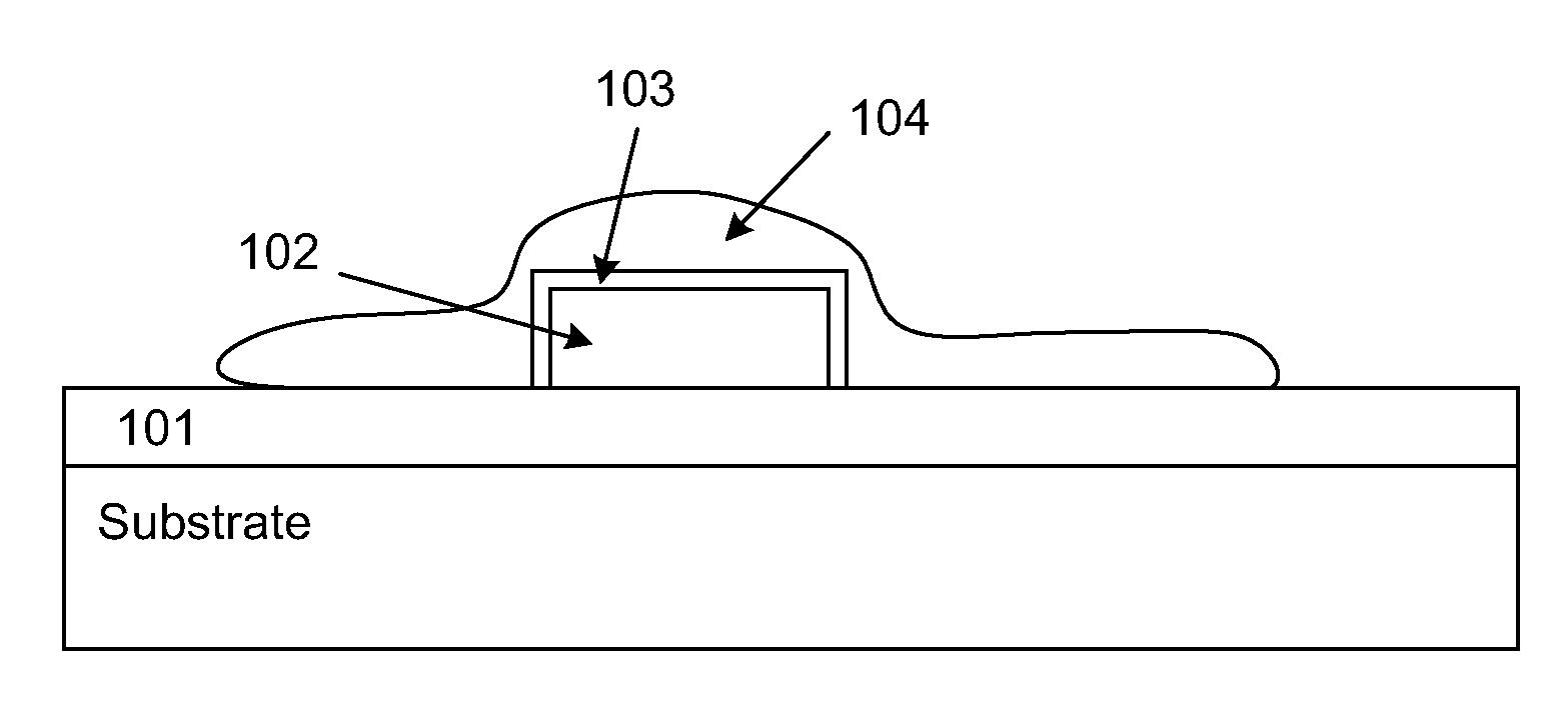
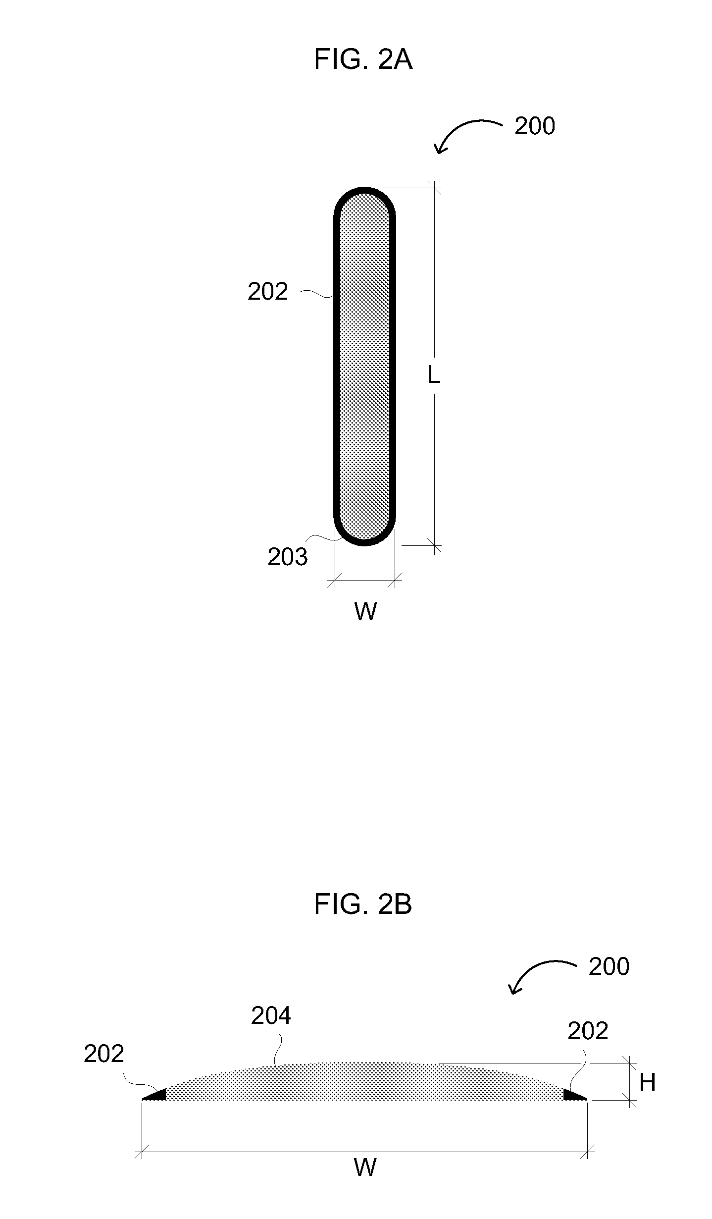
[0031]Reference will now be made in detail to certain embodiments of the invention, examples of which are illustrated in the accompanying drawings. While the invention will be described in conjunction with preferred embodiments, it will be understood that they are not intended to limit the invention to these embodiments. On the contrary, the invention is intended to cover alternatives, modifications and equivalents that may be included within the spirit and scope of the invention as defined by the appended claims. Furthermore, in the following disclosure, numerous specific details are given to provide a thorough understanding of the invention. However, it will be apparent to one skilled in the art that the present invention may be practiced without these specific details. In other instances, well-known methods, procedures, components, and circuits have not been described in detail, to avoid unnecessarily obscuring aspects of the present invention.

[0032]In the present invention, the ...


PUM

PropertyMeasurementUnit
Percent by massaaaaaaaaaa
Viscosityaaaaaaaaaa
Thicknessaaaaaaaaaa

Abstract

The present invention relates to electrically active devices (e.g., capacitors, transistors, diodes, floating gate memory cells, etc.) having dielectric, conductor, and/or semiconductor layers with smooth and/or dome-shaped profiles and methods of forming such devices by depositing or printing (e.g., inkjet printing) an ink composition that includes a semiconductor, metal, or dielectric precursor. The smooth and/or dome-shaped cross-sectional profile allows for smooth topological transitions without sharp steps, preventing feature discontinuities during deposition and allowing for more complete step coverage of subsequently deposited structures. The inventive profile allows for both the uniform growth of oxide layers by thermal oxidation, and substantially uniform etching rates of the structures. Such oxide layers may have a uniform thickness and provide substantially complete coverage of the underlying electrically active feature. Uniform etching allows for an efficient method of reducing a critical dimension of an electrically active structure by simple isotropic etch.

Description

RELATED APPLICATIONS[0001]This application claims the benefit of U.S. Provisional Patent Application No. 60 / 997,335, filed Oct. 1, 2007 (Attorney Docket No. IDR1573), incorporated herein by reference in its entirety.FIELD OF THE INVENTION[0002]The present invention concerns devices such as thin film capacitors, diodes (e.g., a Schottky diode), thin film transistors, and floating gate memory cells comprising a printed, smooth and / or dome-shaped semiconductor thin film feature. The present application discloses structures that can be manufactured using novel ink compositions and novel uses of low-cost printing technology. Exemplary process flows are described in U.S. patent application Ser. Nos. 11 / 818,078, 11 / 888,949, 11 / 888,942, and 12 / 114,741 (Attorney Docket Nos. IDR0813, IDR0742, IDR0743, and IDR1102, respectively), filed on Jun. 12, 2007, Aug. 3, 2007, Aug. 3, 2007, and May 2, 2008, respectively, the relevant portions of which are incorporated herein by reference. Embodiments of...

Claims


Application Information

Patent Timeline
IPC IPC(8): H01L29/788H01L29/786H01L29/00H01L21/208
CPCC23C18/08H01L27/1292C23C18/1245C23C18/1295H01L21/02532H01L21/02601H01L21/02628H01L21/28273H01L21/28518H01L21/288H01L21/76871H01L21/76895H01L29/0657H01L29/66143H01L29/6675H01L29/7881H01L29/872H05K1/16H05K1/162H05K3/125H05K2201/098H01L21/36H01L28/40H01L27/1285C23C18/122H01L29/40114
Inventor KAMATH, ARVINDSCHER, ERIKSMITH, PATRICKCHANDRA, ADITIMOLESA, STEVEN
Owner ENSURGE MICROPOWER ASA
Why Eureka
Try Eureka