Quantum Photonic Imagers and Methods of Fabrication Thereof

a quantum photonic imager and imager technology, applied in static indicating devices, semiconductor lasers, instruments, etc., can solve the problems of increasing the cost of the display system, reducing the efficiency of the light source, and adding complexity and cost to the overall display system

Active Publication Date: 2009-04-02
OSTENDO TECH INC
View PDF34 Cites 147 Cited by
  • Summary
  • Abstract
  • Description
  • Claims
  • Application Information

AI Technical Summary

Problems solved by technology

Being passive imagers, such devices require complex illumination optics and end up wasting a significant part of the generated light, which degrades the performance and increases the cost of the display system.
In effect, a typical prior art reflective imager can only modulate the intensity of the light coupled onto its pixelated reflective surface, a limitation which causes a great deal of inefficiency in utilizing the luminous flux generated by the light source 130, introduces artifacts on the generated image, adds complexities and cost to the overall display system and introduces yet another source of inefficiency in utilizing the light generated by the light source 130.
Furthermore, both the reflective as well as the transmissive type imagers suffer from an effect known as “photonic leakage” which causes light to leak onto the off-state pixels, which significantly limits the contrast and black levels that can be achieved by these types of imagers.
[1]-[4]) for use in projectors 100 of FIG. 1A to illuminate reflective imagers 110 such as the micro-mirror imager device, the use of semiconductor laser diodes as a light source does not help in overcoming any of the drawbacks of prior art imagers discussed above.
[7] would be a small fraction of that provided by the pumping light source, which, being an OLED based light source, would not likely to offer an ample amount of light, rendering the brightness generated by the laser projector of prior art Ref.
[7] hardly sufficient to be of practical use in most projection display applications.
[8]-[30]), no prior art was found that teaches the use of multicolor laser emitters as pixels in an imager device.
[22], the approach described would tend to produce substantially large pixels size because of the inherent size of the multiple color of VCSEL diodes it uses which are arranged side-by-side in the same plane to form a pixel array, rendering it not usable as an imager device.

Method used


Image

  • Quantum Photonic Imagers and Methods of Fabrication Thereof
  • Quantum Photonic Imagers and Methods of Fabrication Thereof
  • Quantum Photonic Imagers and Methods of Fabrication Thereof

Examples


first embodiment

of the Vertical Waveguides

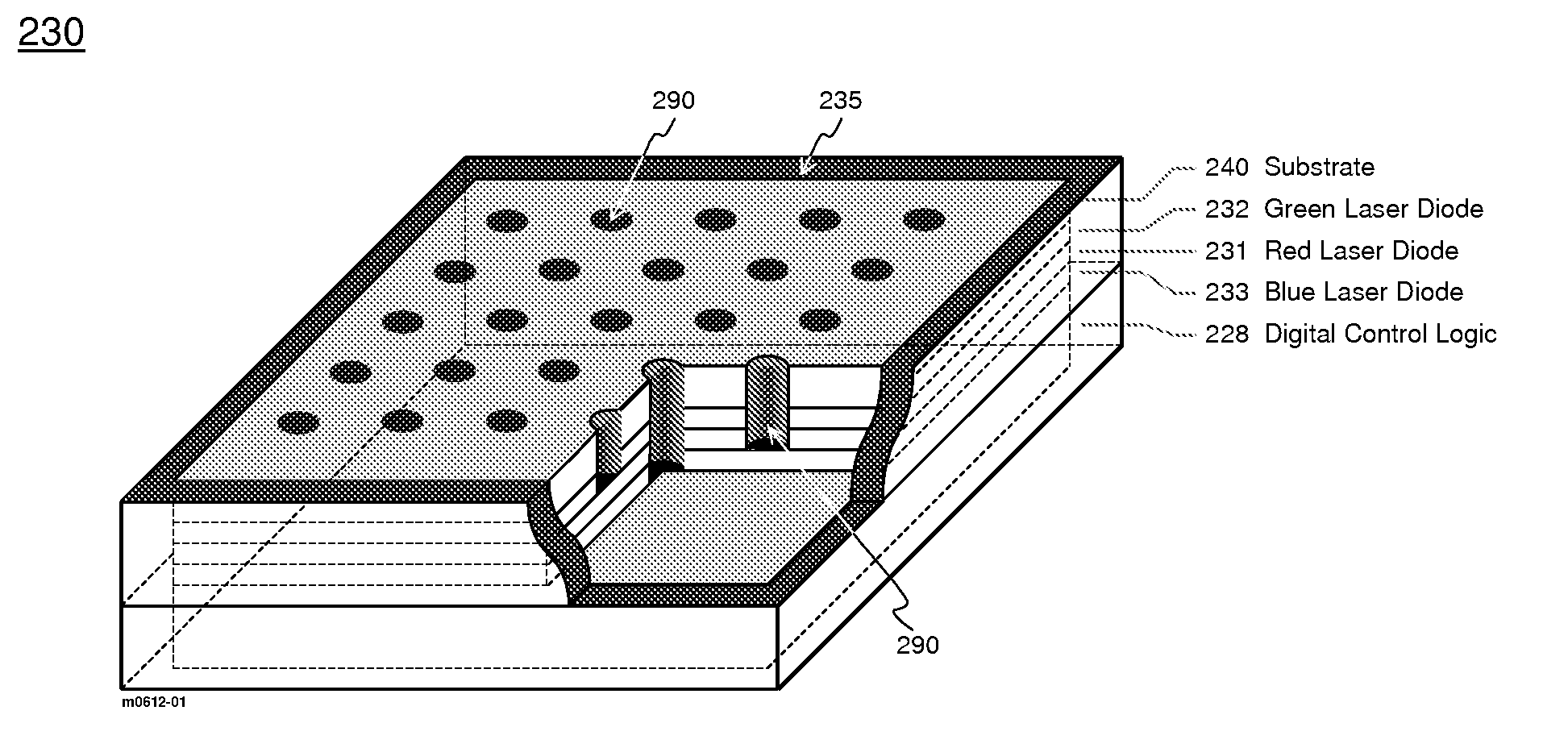
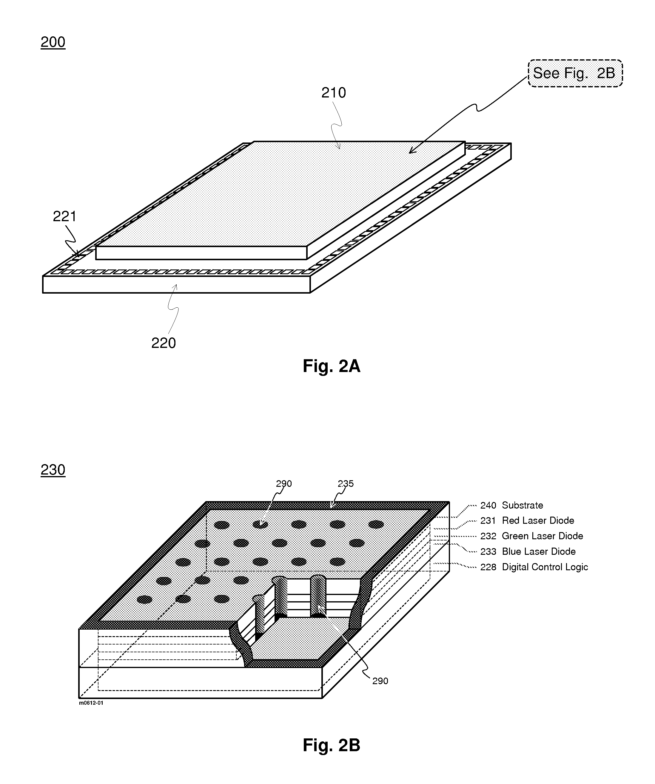
[0153]In one embodiment of the Quantum Photonic Imager device 200 of this invention the cores 291 of the pixel's vertical waveguides 290 would be “evanescence field coupled” to the optical confinement regions of stacked laser diodes 231, 232, and 233 that form a single pixel 230. In this embodiment the vertical waveguide cladding 292 would be comprised of an outer layer 293 of 50-nm to 100-nm thick of insulating material, such as SiO2, and an inner layer 294 of highly reflective metal such as aluminum (Al), silver (Ag) or gold (Au). The core 291 of the vertical waveguides 290 could either be air-filled or filled with a dielectric material such as SiO2, silicon nitride (Si3N4) or tantalum pentoxide (TaO5). Through the evanescence field coupling of this embodiment, a fraction of the laser light confined within the optical confinement region of each of the laser diodes 231, 232, and 233 would be coupled into the dielectric core 291 of the vertical waveguides 2...

second embodiment

of the Vertical Waveguides

[0158]In another embodiment of the Quantum Photonic Imager device 200 of this invention the cores 291 of the pixel's vertical waveguides 290 would be coupled to the optical confinement regions of stacked laser diodes 231, 232, and 233 that form a single pixel 230 through the use of anisotropic multilayer thin cladding. What is meant by “anisotropic” in this context is that the reflectance / transmittance characteristics would be asymmetric at either side of the interface between the vertical waveguide 290 and the optical confinement regions of the stacked laser diodes 231, 232, and 233. The simplest realization of this embodiment would be to use a single thin cladding layer 293 having a refractive index value between that of the waveguide core 291 and the optical confinement regions of laser diodes 231, 232, and 233 and having the waveguide core 291 preferably filled with a dielectric material preferably having a refractive index that is at least equal to tha...


PUM


Abstract

Emissive quantum photonic imagers comprised of a spatial array of digitally addressable multicolor pixels. Each pixel is a vertical stack of multiple semiconductor laser diodes, each of which can generate laser light of a different color. Within each multicolor pixel, the light generated from the stack of diodes is emitted perpendicular to the plane of the imager device via a plurality of vertical waveguides that are coupled to the optical confinement regions of each of the multiple laser diodes comprising the imager device. Each of the laser diodes comprising a single pixel is individually addressable, enabling each pixel to simultaneously emit any combination of the colors associated with the laser diodes at any required on/off duty cycle for each color. Each individual multicolor pixel can simultaneously emit the required colors and brightness values by controlling the on/off duty cycles of their respective laser diodes.

Description

CROSS-REFERENCE TO RELATED APPLICATION[0001]This application claims the benefit of U.S. Provisional Patent Application No. 60 / 975,772 filed Sep. 27, 2007.BACKGROUND OF THE INVENTION[0002]1. Field of the Invention[0003]The present invention relates to emissive imager devices comprising a monolithic semiconductor arrays of multicolor laser emitters that can be used as an image sources in digital projection systems.[0004]2. Prior Art[0005]The advent of digital display technology is causing a phenomenal demand for digital displays. Several display technologies are poised to address this demand; including Plasma Display Panel (PDP), Liquid Crystal Display (LCD), and imager based projection displays that use micro-mirrors, a liquid crystal on silicon (LCOS) device or a high temperature poly-silicon (HTPS) device (Ref. [33]). Of particular interest to the field of this invention are projection based displays that use imager devices, such as those mentioned, as an image forming device. Thes...

Claims


Application Information

Patent Timeline
Patent Type & Authority Applications(United States)
IPC IPC(8): G03B21/14G09G3/32H01L33/00H01S5/18
CPCH01S5/4043H01S5/105H01S5/2009H04N9/3197H01S5/4093H01S5/34333H01S5/34326H01S5/18H04N9/3161B82Y20/00H01S5/3063H01S5/02345H01S5/11G09G3/2018G09G3/32G09G2300/0842G09G2310/0235G09G2340/06H01S5/183
Inventor EL-GHOROURY, HUSSEIN S.BROWN, ROBERT G.W.MCNEILL, DALE A.DENBOER, HUIBERTLANZONE, ANDREW J.
Owner OSTENDO TECH INC
Why Eureka
Try Eureka