Dual damascene with amorphous carbon for 3D deep via/trench application

a technology of amorphous carbon and damascene, which is applied in the direction of diodes, semiconductor devices, electrical apparatus, etc., can solve the problems of difficult etching of relatively deep vias and trenches between layers, insufficient conventional fabrication techniques, and inability to meet the requirements of 3d integrated circuits

Active Publication Date: 2009-04-02
SANDISK CORP +1
View PDF27 Cites 179 Cited by
  • Summary
  • Abstract
  • Description
  • Claims
  • Application Information

AI Technical Summary

Benefits of technology

[0005]The present invention addresses the above and other issues by providing a method for fabricating a 3-D monolithic memory device in which etching of vias and trenches is improved.

Problems solved by technology

However, various challenges are encountered in forming interconnects between the layers of such memory devices and other 3-D integrated circuits.
In particular, as 3-D monolithic integrated circuits push minimum feature sizes and etch and fill aspect ratios to the limit, conventional fabrication techniques have been found to be inadequate.
For example, etching of relatively deep vias and trenches between layers can be problematic.

Method used


Image

  • Dual damascene with amorphous carbon for 3D deep via/trench application
  • Dual damascene with amorphous carbon for 3D deep via/trench application
  • Dual damascene with amorphous carbon for 3D deep via/trench application

Examples


Embodiment Construction

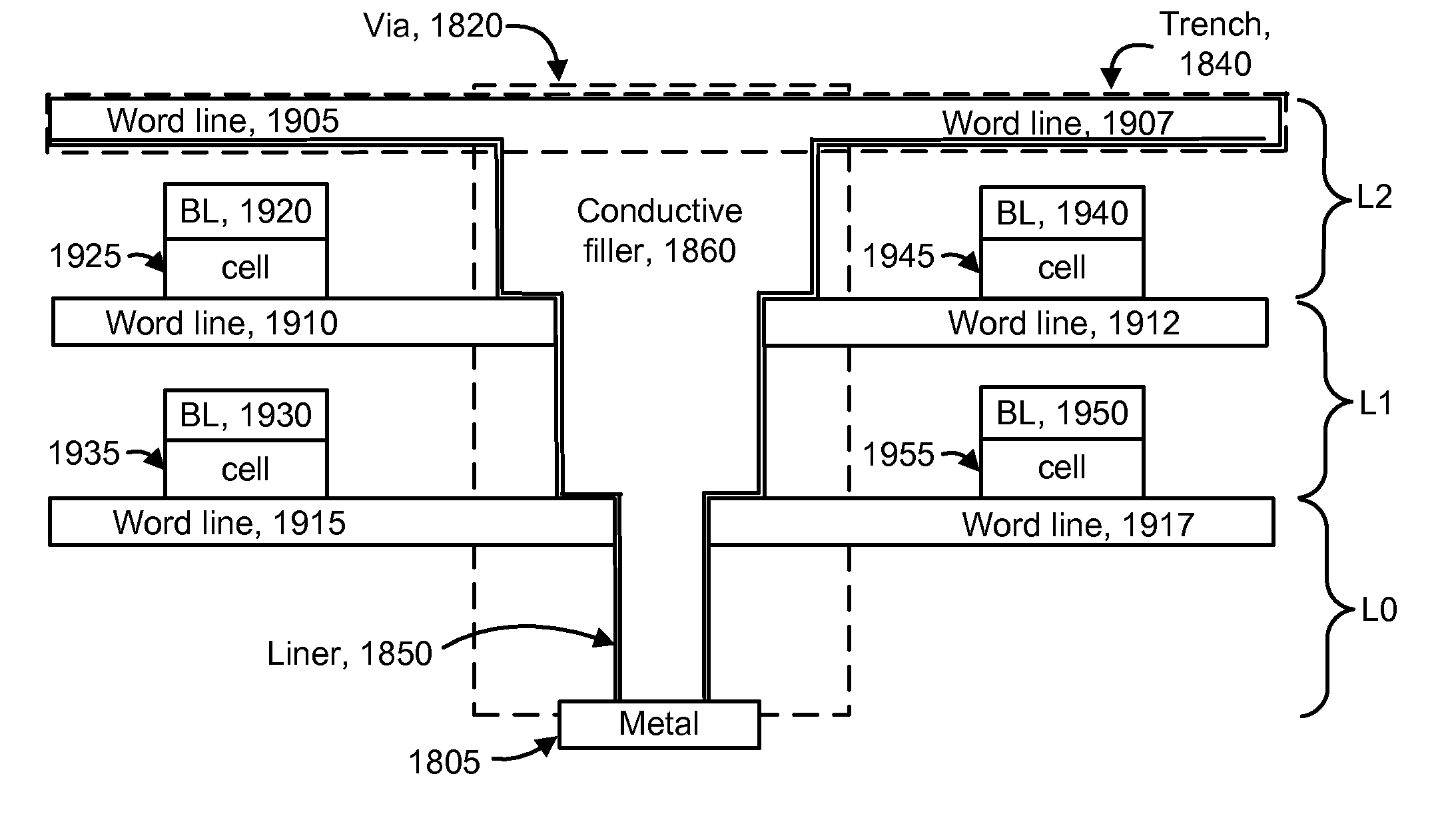
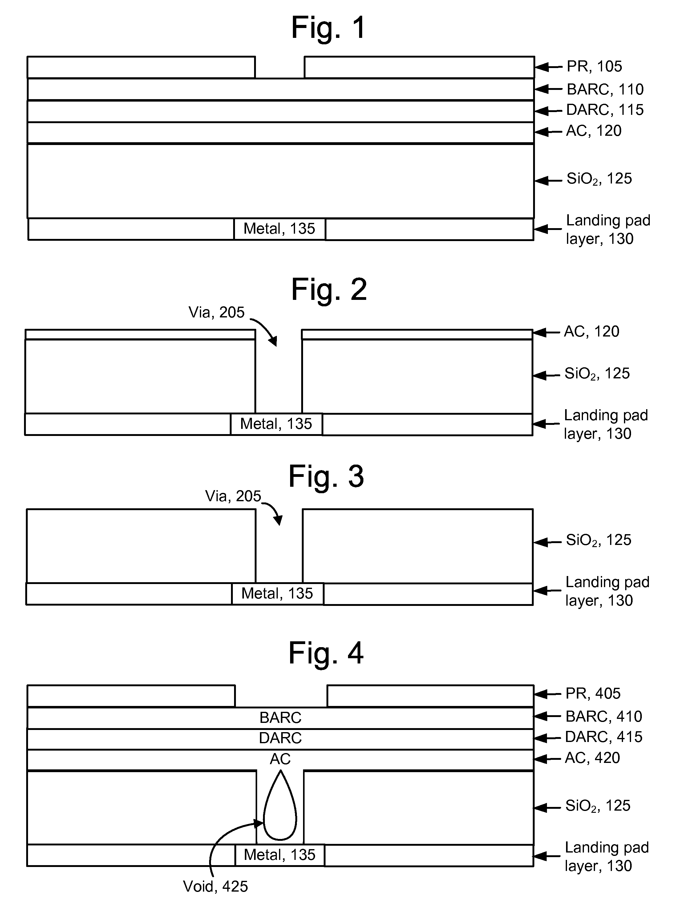
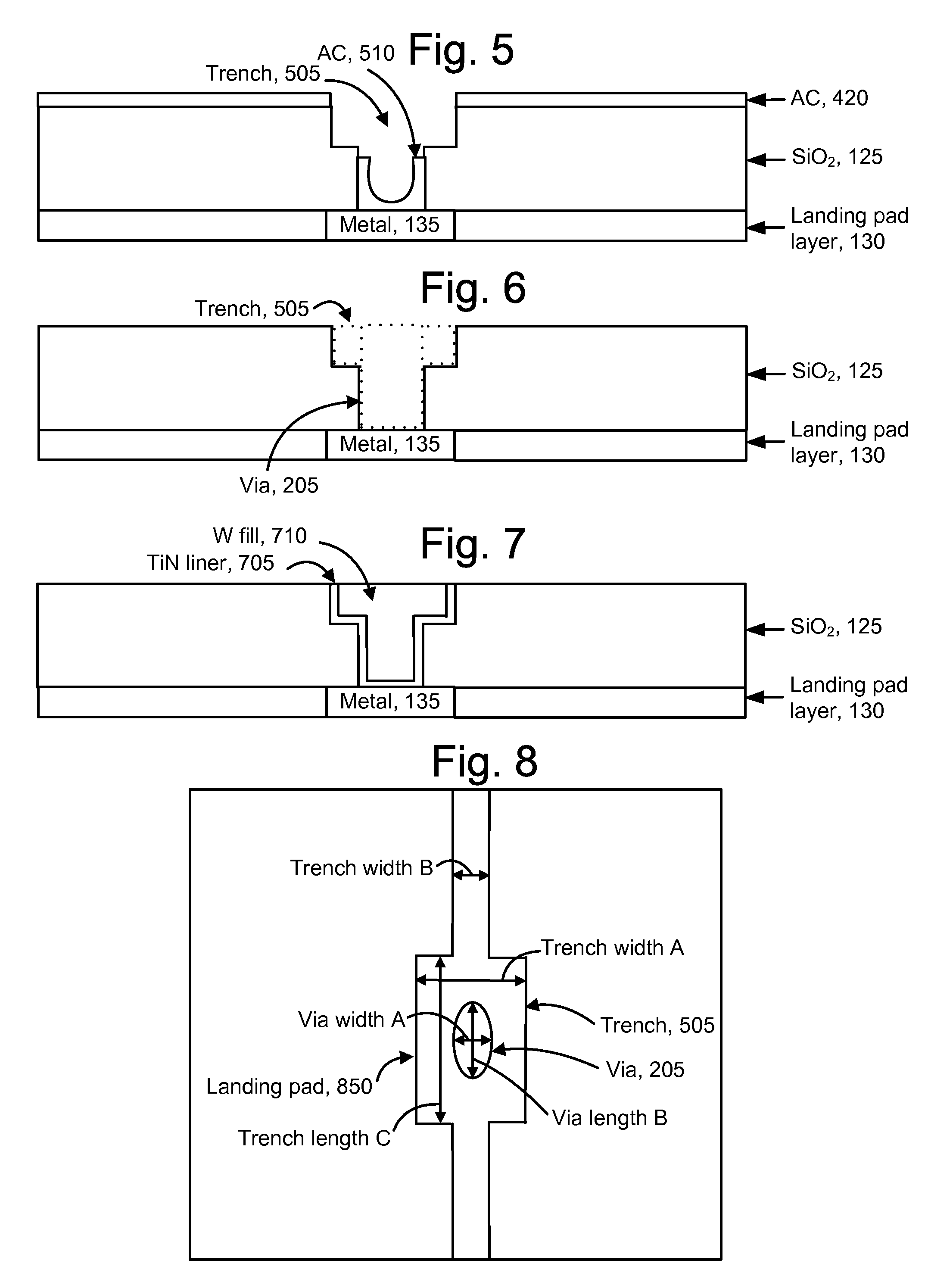
[0032]The present invention provides a method for fabricating a 3-D monolithic memory device in which etching of vias and trenches is improved. A corresponding apparatus is also provided.

[0033]The following acronyms and abbreviations are used:[0034]AC—amorphous carbon;[0035]BARC—bottom antireflective coating, available from Brewer Science, Rolla, Mo.[0036]DARC—dielectric antireflective coating; and[0037]PR—photoresist.

[0038]As mentioned at the outset, etching of relatively deep vias and trenches between layers in a 3-D monolithic memory device can be problematic. A monolithic three dimensional memory array or device is one in which multiple memory levels are formed above a single substrate, such as a wafer, with no intervening substrates. The layers forming one memory level are deposited or grown directly over the layers of an existing level or levels. In contrast, stacked memories have been constructed by forming memory levels on separate substrates and adhering the memory levels a...


PUM


Abstract

A method for fabricating a 3-D monolithic memory device in which a via and trench are etched using an amorphous carbon hard mask. The via extends in multiple levels of the device as a multi-level vertical interconnect. The trench extends laterally, such as to provide a word line or bit line for memory cells, or to provide other routing paths. A dual damascene process can be used in which the via is formed first and the trench is formed second, or the trench is formed first and the via is formed second. The technique is particularly suitable for deep via applications, such as for via depths of greater than 1 μm. A dielectric antireflective coating, optionally with a bottom antireflective coating, can be used to etch an amorphous carbon layer to provide the amorphous carbon hard mask.

Description

BACKGROUND OF THE INVENTION[0001]1. Field of the Invention[0002]The present invention relates to fabricating a 3-D integrated circuit.[0003]2. Description of the Related Art[0004]Due to the high cost of silicon real estate and the need to create ever smaller memory devices, monolithic 3-D memory devices have become increasingly popular. Such devices can include multiple levels of interconnected memory cells. Examples of this technology can be found in U.S. 2005 / 0098800, titled “Nonvolatile memory cell comprising a reduced height vertical diode,” published May 12, 2005, and U.S. Pat. No. 6,952,030, titled “High-density three-dimensional memory cell”, issued Oct. 4, 2005, both of which are incorporated herein by reference. In such devices, the memory cells can be formed as diodes in polysilicon layers, while conductive rails which interconnect the memory cells can be formed by etching oxide layers and depositing a conductive material. However, various challenges are encountered in for...

Claims


Application Information

Patent Timeline
Patent Type & Authority Applications(United States)
IPC IPC(8): H01L21/4763
CPCH01L21/31144H01L27/1021H01L27/101H01L21/76808
Inventor RAGHURAM, USHAKONEVECKI, MICHAEL W.
Owner SANDISK CORP
Why Eureka
Try Eureka