

Organic electroluminescent device, display, and illuminating device
a technology of electroluminescent elements and lighting devices, applied in the direction of organic semiconductor devices, discharge tubes luminescnet screens, other domestic articles, etc., can solve the problems of poor emission lifetime of elements compared to conventional elements, inability to achieve a level of practical use, and difficulty in preparing such elements via coating methods, etc., to achieve long light emission life and high light emission efficiency
- Summary
- Abstract
- Description
- Claims
- Application Information
AI Technical Summary
Benefits of technology
Problems solved by technology
Method used
Image

Examples
example 1
Preparation of Organic EL Elements 1-1 through 13
[0165]After applying patterning to a substrate (NA45, produced by NH Techno Glass Corp.) which was treated in such a way that ITO (indium tin oxide), as an anode, was applied onto a 100 mm×100 mm×1.1 mm glass substrate to form a 100 nm film, the transparent substrate provided with the above transparent ITO electrode was subjected to ultrasonic cleaning employing isopropyl alcohol, was dried in desiccated nitrogen gas, and was subjected to UV ozone cleaning for 5 minutes. The resulting transparent substrate was adhered onto the substrate holder of a commercial vacuum deposition apparatus. On the other hand, 200 mg of α-NPD was placed in a molybdenum resistance heating boat, 200 mg of CBP as a host compound was placed in another molybdenum resistance heating boat, 200 mg of basocuproin (BCP) was placed in further another molybdenum resistance heating boat, 100 mg of Ir-12 was placed in still another molybdenum resistance heating boat, a...
example 2
Preparation of Organic EL Full-Color Display Device
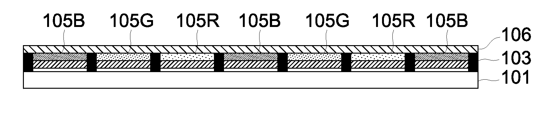
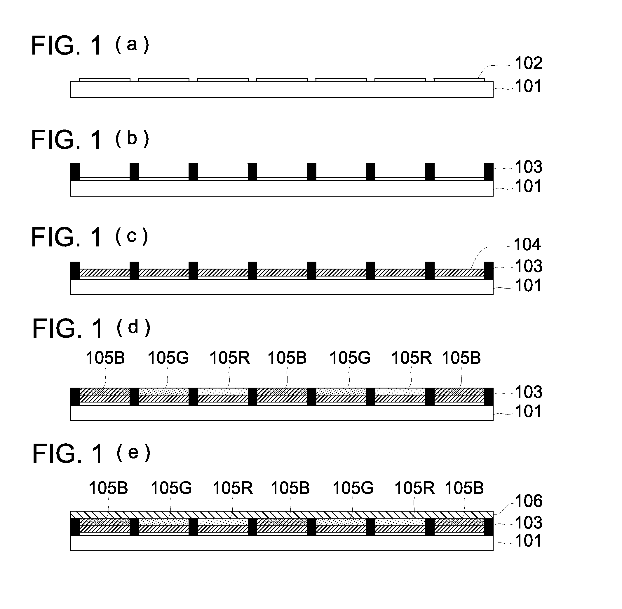
[0177]FIG. 1 is a schematic constitutional view of an organic EL full-color display device. After applying patterning at a pitch of 100 μm to a substrate (NA45, produced by NH Techno Glass Corp.) which was treated in such a manner that an ITO transparent electrode (102) as an anode was applied onto glass substrate 101 to form a 100 nm film, non-photosensitive partition wall 103 (at a width of 20 μm and a thickness of 2.0 μm) was formed between the ITO transparent electrodes on the above glass substrate via photolithography. The positive hole injecting layer composition of the following formula was injected into the space between the polyimide partition walls on the ITO electrode by employing an ink-jet head (MJ800C, produced by Epson Corp.), followed by a drying process at 200° C. over 10 minutes, whereby positive hole injecting layer 104 was prepared. Onto the resulting positive hole injecting layer discharged was each of the follo...
example 3
Preparation of Organic EL Element 3-1
[0180]After applying patterning to a substrate (NA45, produced by NH Techno Glass Corp.) which was treated in such a manner that ITO (indium tin oxide), as an anode, was applied onto a 100 mm×100 mm×1.1 mm glass substrate to form a 100 nm film, the transparent substrate provided with the above ITO transparent electrode was subjected to ultrasonic cleaning employing isopropyl alcohol, dried in desiccated nitrogen gas, and subjected to UV ozone cleaning over 5 minutes. The resulting substrate was mounted in a commercial spin coater and subjected to spin coating (at a film thickness of about 40 nm) under the conditions of 1,000 rpm and 30 seconds, employing a solution prepared by dissolving 60 mg of PVK in 10 ml of 1,2-dichloroethane, followed by drying under vacuum at 60° C. for one hour, whereby a positive hole transporting layer was prepared.
[0181]Subsequently, spin coating (at a film thickness of about 40 nm) was carried out at the conditions of...
PUM
| Property | Measurement | Unit |
|---|---|---|
| Percent by mass | aaaaa | aaaaa |
| Percent by mass | aaaaa | aaaaa |
| Percent by mass | aaaaa | aaaaa |
Abstract
Description
Claims
Application Information