Organic Thin Film Transistors

Inactive Publication Date: 2009-04-23
CAMBRIDGE DISPLAY TECH LTD +1
View PDF14 Cites 9 Cited by
  • Summary
  • Abstract
  • Description
  • Claims
  • Application Information

AI Technical Summary

Benefits of technology

[0029]In one particularly preferred embodiments, the wetting and anti-wetting material form a phase separated mixture. For example, the phase separated mixture may comprise wetting material dissolved in a first solvent and anti-wetting material dissolved in a second solvent, the first and second solvents being immiscible. This embodiment provides a good way of defining wetting domains in an anti-wetting matrix. The mixture may also comprise a surfactant. A surfactant can be utilized to control the size of the wetting domains.
[0030]One or both of the wetting domains and the anti-wetting matrix may comprise molecules having attachment groups which attach the molecules to the surface onto which the organic semiconductor is deposited. This will serve to anchor the seeding molec

Problems solved by technology

As stated previously, the present inventors have realised that it may not be desirable to increase the crystallinity, and thus the conductivity, of the organic semiconductor i

Method used


Image

  • Organic Thin Film Transistors
  • Organic Thin Film Transistors
  • Organic Thin Film Transistors

Examples


Embodiment Construction

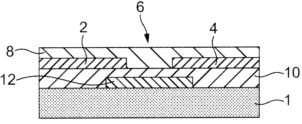
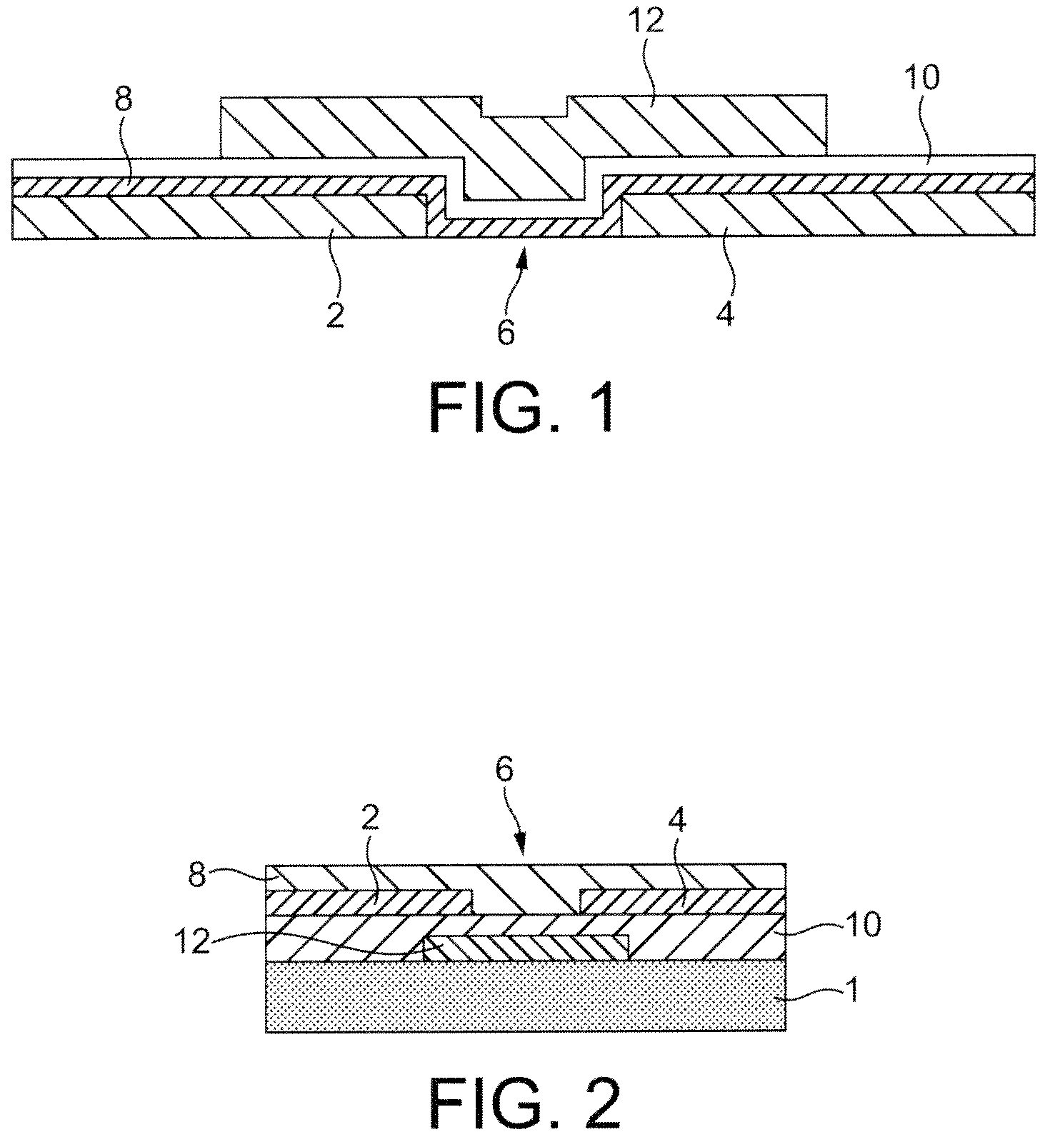
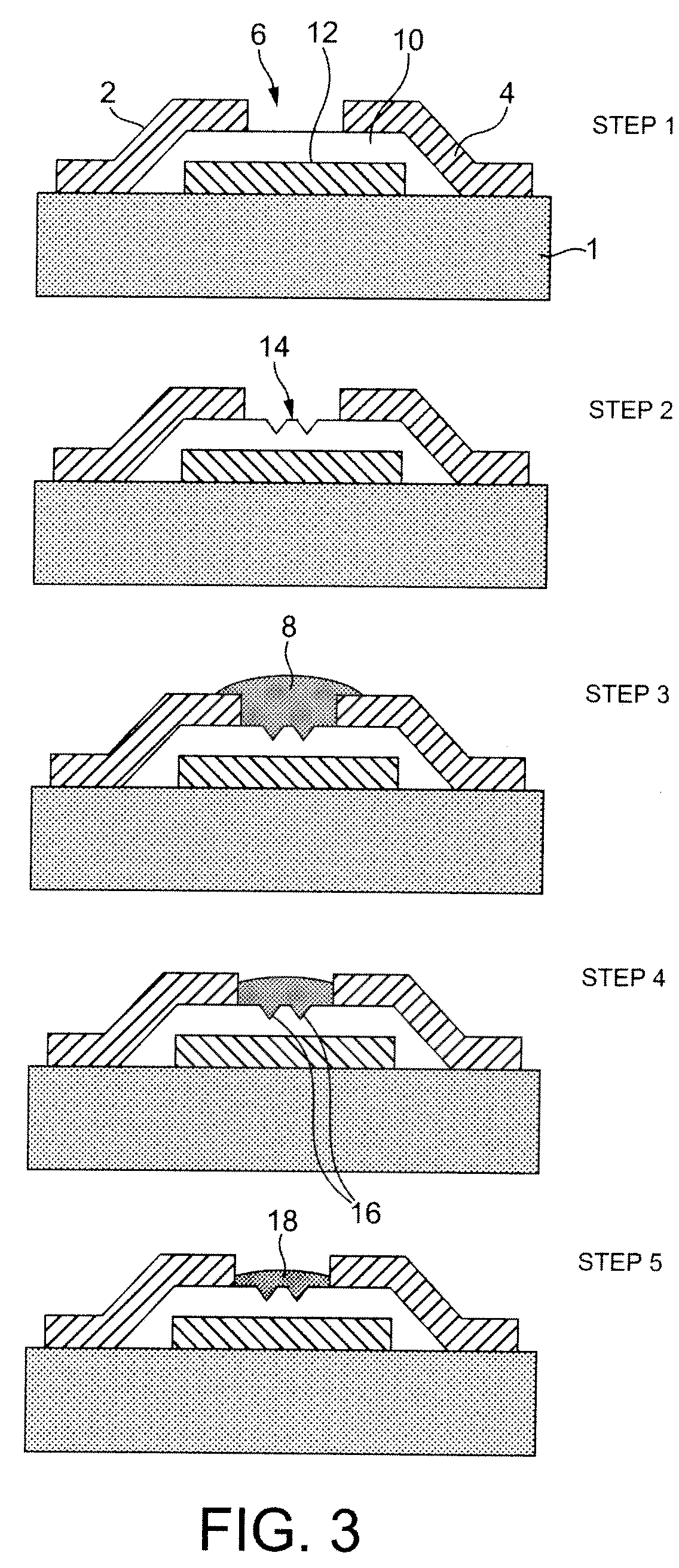
[0042]An example method of how this technique may be carried out is shown schematically in FIG. 3.

[0043]In step 1, a substrate 1 is initially prepared by formation of a gate electrode 12, a dielectric layer 10, and source and drain contacts 2, 4 thereon (this is a bottom gate, bottom contact transistor architecture).

[0044]The electrodes can be printed or deposited using other simple patterning techniques which are known in the art.

[0045]The dielectric material may be solution processable. For example, the dielectric layer may be an organic photoresist such as a polyimide which can be readily spin coated and patterned. Alternatively, the dielectric layer may be an inorganic material such as SiO2.

[0046]In step 2, the exposed surface of the dielectric layer in the channel region is treated to form crystallization sites. In the embodiment shown in FIG. 3, a physical seeding method is utilized in which the surface is stamped to form ordered nano-indentations 14. Methods for indenting the...


PUM


Abstract

A method of forming an organic thin film transistor comprising source and drain electrodes with a channel region therebetween, a gate electrode, a dielectric layer disposed between the source and drain electrodes and the gate electrode, and an organic semiconductor disposed in at least the channel region between the source and drain electrodes, said method comprising: seeding a surface in the channel region with crystallization sites prior to deposition of the organic semiconductor; and depositing the organic semiconductor onto the seeded surface whereby the organic semiconductor crystallizes at the crystallization sites forming crystalline domains in the channel region.

Description

FIELD OF INVENTION[0001]The present invention relates to organic thin film transistors.BACKGROUND OF THE INVENTION[0002]Transistors can be divided into two main types: bipolar junction transistors and field-effect transistors. Both types share a common structure comprising three electrodes with a semi-conductive material disposed therebetween in a channel region. The three electrodes of a bipolar junction transistor are known as the emitter, collector and base, whereas in a field-effect transistor the three electrodes are known as the source, drain and gate. Bipolar junction transistors may be described as current-operated devices as the current between the emitter and collector is controlled by the current flowing between the base and emitter. In contrast, field-effect transistors may be described as voltage-operated devices as the current flowing between source and drain is controlled by the voltage between the gate and the source.[0003]Transistors can also be classified as P-type...

Claims


Application Information

Patent Timeline
IPC IPC(8): H01L51/40H01L51/10
CPCH01L51/0516H01L51/0558H01L51/0545H01L51/0541H10K10/468H10K10/464H10K10/484H10K10/466H10K71/191H10K10/462
Inventor HALLS, JONATHAN J.MURPHY, CRAIGWHITING, GREGORYHOTTA, SADAYOSHI
Owner CAMBRIDGE DISPLAY TECH LTD
Why Eureka
Try Eureka