Semiconductor device and method for manufacturing semiconductor device

a semiconductor and semiconductor technology, applied in the direction of instruments, optics, transistors, etc., can solve the problems of significant challenges in the reduction of the number of photomasks, the decrease of the throughput of the manufacturing process of amorphous semiconductor tfts, and the increase of the manufacturing cost of the manufacturing process. , to achieve the effect of reducing the time of manufacture and manufacturing cost, and improving the aperture ratio

Active Publication Date: 2009-04-23
SEMICON ENERGY LAB CO LTD
View PDF46 Cites 30 Cited by
  • Summary
  • Abstract
  • Description
  • Claims
  • Application Information

AI Technical Summary

Benefits of technology

[0041]With such a structure, an active matrix substrate can be manufactured by three photolithography processes using two photomasks. Accordingly, as compared with an amorphous semiconductor TFT conventionally manufactured by at least four times of photolithography processes using four photomasks, the number of photomasks and the number of photolithography processes can be significantly reduced, and time of manufacture and manufacturing cost can be reduced.
[0042]In accordance with the present invention, an active matrix substrate can be manufactured by three photolithography processes using two photomasks. Accordingly, as compared with an amorphous semiconductor TFT conventionally manufactured by at least four times of photolithography processes using four photomasks, the number of photomasks and the number of photolithography processes can be significantly reduced, and time of manufacture and manufacturing cost can be reduced.
[0043]In accordance with the present invention, a source / drain electrode and a source / drain wiring are formed using a second conductive layer having a layered structure of a transparent conductive layer and a metal layer; therefore, a region where contact holes for a source / drain electrode and a pixel electrode, which is conventionally in a pixel portion is not required; therefore, aperture ratio can be improved. Further, with such a structure that a pixel electrode is in contact with a substrate and is not stacked with an insulating film, aperture ratio and transmittance of pixels are improved.

Problems solved by technology

Therefore, in the case of manufacturing an amorphous semiconductor TFT using conventional five masks, a photolithography process is to be repeated five times. A photolithography process having a plurality of steps of exposure, development, and the like have become a factor greatly affecting decrease in throughput and increase in manufacturing cost of a manufacturing process of amorphous semiconductor TFTs.
Therefore, reduction in the number of photomasks is a significant challenge for producing semiconductor devices using lower cost amorphous semiconductor TFTs.

Method used


Image

  • Semiconductor device and method for manufacturing semiconductor device
  • Semiconductor device and method for manufacturing semiconductor device
  • Semiconductor device and method for manufacturing semiconductor device

Examples


embodiment mode 1

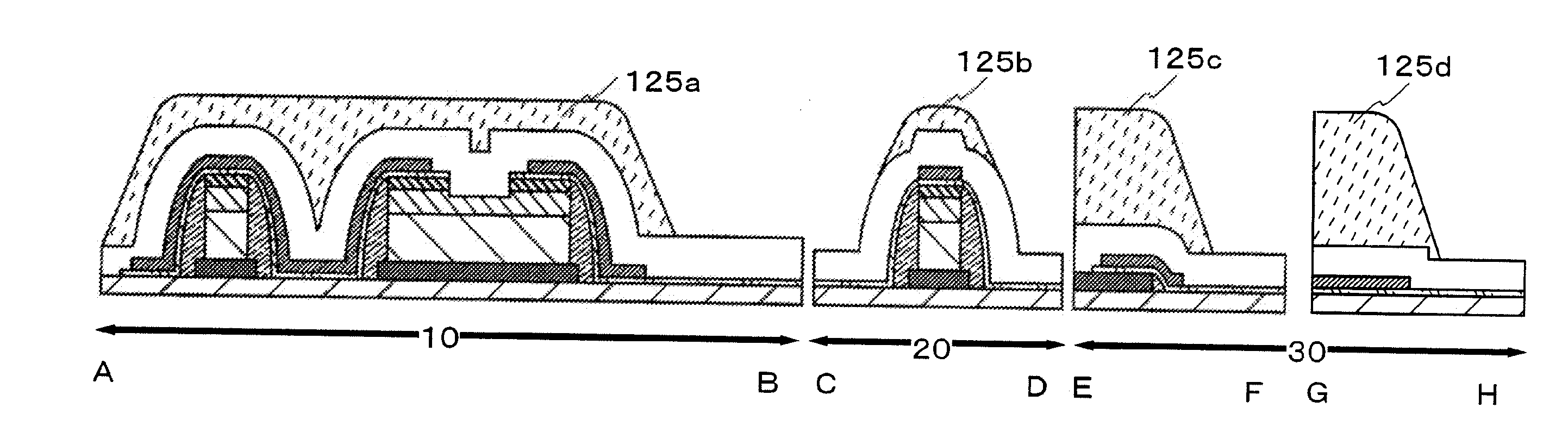
[0059]FIG. 1 is a plan view illustrating an example of an active matrix substrate having amorphous semiconductor TFTs of the present invention; here, the structure of one pixel among a plurality of pixels arranged in matrix is shown for simplicity.

[0060]As shown in FIG. 1, an active matrix substrate having amorphous semiconductor TFTs has a plurality of gate wirings 103a which are arranged in parallel to each other, and source wirings 119a arranged in parallel to each other, which are arranged perpendicularly to the gate wirings 103a.

[0061]Further, the pixel electrode 115f is placed in a region surrounded by the gate wiring 103a and the source wiring 119a. The pixel electrode 115f is formed of the same material as the transparent conductive layer 115b of the source / drain electrode 119b.

[0062]Further, a capacitor line 103b is provided between two adjacent gate wirings below the pixel electrode 115f, in parallel with the gate wirings. The capacitor line 103b is provided in every pix...

embodiment mode 2

[0105]In Embodiment Mode 1, a TFT using an amorphous semiconductor layer is described; however, in this embodiment mode, an example of a TFT using a microcrystalline semiconductor layer will be described. A schematic diagram of a TFT using a microcrystalline semiconductor is shown in FIG. 9. In this embodiment mode, a stack of a first microcrystalline semiconductor layer 126 and a first amorphous semiconductor layer 127 is used instead of the first amorphous semiconductor layer 106 in Embodiment Mode 1.

[0106]The first microcrystalline semiconductor layer 126 serves as a channel. This first microcrystalline semiconductor layer 126 can be formed by high frequency plasma CVD with a frequency of several tens of MHz to several hundreds of MHz or by microwave plasma CVD with a frequency of I GHz or more. Typically, the microcrystalline semiconductor layer can be formed using silicon hydride such as SiH4 or Si2H6 which is diluted with hydrogen. Further, the microcrystalline semiconductor f...

embodiment mode 3

[0108]In this embodiment mode, an example of using a positive photosensitive resin is used instead of the third photoresist patterns 124a to 124d in the third photolithography process of Embodiment Mode 1 will be described. A schematic diagram of a TFT using the positive photosensitive resin is shown in FIG. 10.

[0109]In the third photolithography process in Embodiment Mode 1, a positive photosensitive material is formed, and exposure is performed from the rear surface of the substrate 101. Using the fact that a portion corresponding to the first conductive layer patterned by first photolithography process and the metal layer patterned by second photolithography process in Embodiment Mode 1 is shielded from light, a positive photosensitive material pattern 129 is formed. At the time of forming the positive photosensitive material pattern 129, using the first conductive layer and the metal layer which are formed over the substrate 101 as masks, exposure is performed from the rear surf...


PUM

PropertyMeasurementUnit
thicknessaaaaaaaaaa
thicknessaaaaaaaaaa
thicknessaaaaaaaaaa

Abstract

A first resist pattern is formed by exposure using a first multi-tone photomask, and a first conductive layer, a first insulating layer, a first semiconductor layer, and a second semiconductor layer are etched, so that an island-shaped single layer and an island-shaped stack are formed. Here, sidewalls are formed on side surfaces of the island-shaped single layer and the island-shaped stack. Further, a second resist pattern is formed by exposure using a second multi-tone photomask, and a second conductive layer and the second semiconductor layer are etched, so that a thin film transistor, a pixel electrode, and a connection terminal are formed. After that, a third resist pattern is formed by exposure from a rear side using metal layers of the first conductive layer and the second conductive layer as masks, and the third insulating layer are etched, so that a protective insulating layer is formed.

Description

BACKGROUND OF THE INVENTION[0001]1. Field of the Invention[0002]The present invention relates to a semiconductor device which has a circuit including a thin film transistor (hereinafter referred to as a TFT) and a method for manufacturing the semiconductor device. For example, the present invention relates to electro-optic devices typified by display devices using a liquid crystal element or a light emitting element, and to electronic devices mounted with those electro-optic devices as a component.[0003]Note that a semiconductor device in this specification refers to all electrical devices which can function by utilizing semiconductor characteristics, and electro-optical devices, semiconductor circuits, and electronic appliances are all semiconductor devices.[0004]2. Description of the Related Art[0005]Most of display devices such as display of liquid crystal televisions, personal computers, and cellular phones that are widely available use liquid crystal display devices utilizing T...

Claims


Application Information

Patent Timeline
Patent Type & Authority Applications(United States)
IPC IPC(8): H01L33/00H01L21/00G02F1/1368H01L21/336H01L29/786
CPCH01L27/1214H01L29/41733H01L29/78678H01L29/78609H01L29/66765H01L27/1288
Inventor HOSOYA, KUNIOFUJIKAWA, SAISHI
Owner SEMICON ENERGY LAB CO LTD
Why Eureka
Try Eureka