Method and system for chemically enhanced laser trimming of substrate edges

a laser cutting and edge technology, applied in the direction of chemistry apparatus and processes, cleaning processes and utensils, cleaning using liquids, etc., can solve the problems of adversely affecting device yield and reliability, and achieve the effects of reducing material amount, increasing device yield, and increasing usable wafer area

Inactive Publication Date: 2009-04-30
SOKUDO CO LTD
View PDF6 Cites 17 Cited by
  • Summary
  • Abstract
  • Description
  • Claims
  • Application Information

AI Technical Summary

Benefits of technology

[0008]According to another embodiment of the present invention, a method of processing material present on a peripheral portion of a topside of a substrate is provided. The method includes placing the substrate on a spin chuck and chucking the substrate to the spin chuck. The method also includes rotating the substrate about an axis of the spin chuck and flowing a chemical onto the peripheral portion of the topside of the substrate. The chemical flows along a radial direction across the topside of the substrate. The method further includes exposing at least a portion of the peripheral portion of the topside of the substrate to incident radiation. The incident radiation enhances a chemical reaction between the chemical and the material. Additionally, the method includes removing at least a portion of the material present on the peripheral portion of the topside of the substrate.
[0010]Many benefits are achieved by way of the present invention over conventional techniques. For example, embodiments of the present invention provide for increases in usable wafer area, which provide for increased device yields. Additionally, embodiments reduce the amount of material contributing to the generation of particles, which adversely impact device yield and reliability. Depending upon the embodiment, one or more of these benefits, as well as other benefits, may be achieved. These and other benefits will be described in more detail throughout the present specification and more particularly below in conjunction with the following drawings.

Problems solved by technology

Additionally, embodiments reduce the amount of material contributing to the generation of particles, which adversely impact device yield and reliability.

Method used


Image

  • Method and system for chemically enhanced laser trimming of substrate edges
  • Method and system for chemically enhanced laser trimming of substrate edges
  • Method and system for chemically enhanced laser trimming of substrate edges

Examples


Embodiment Construction

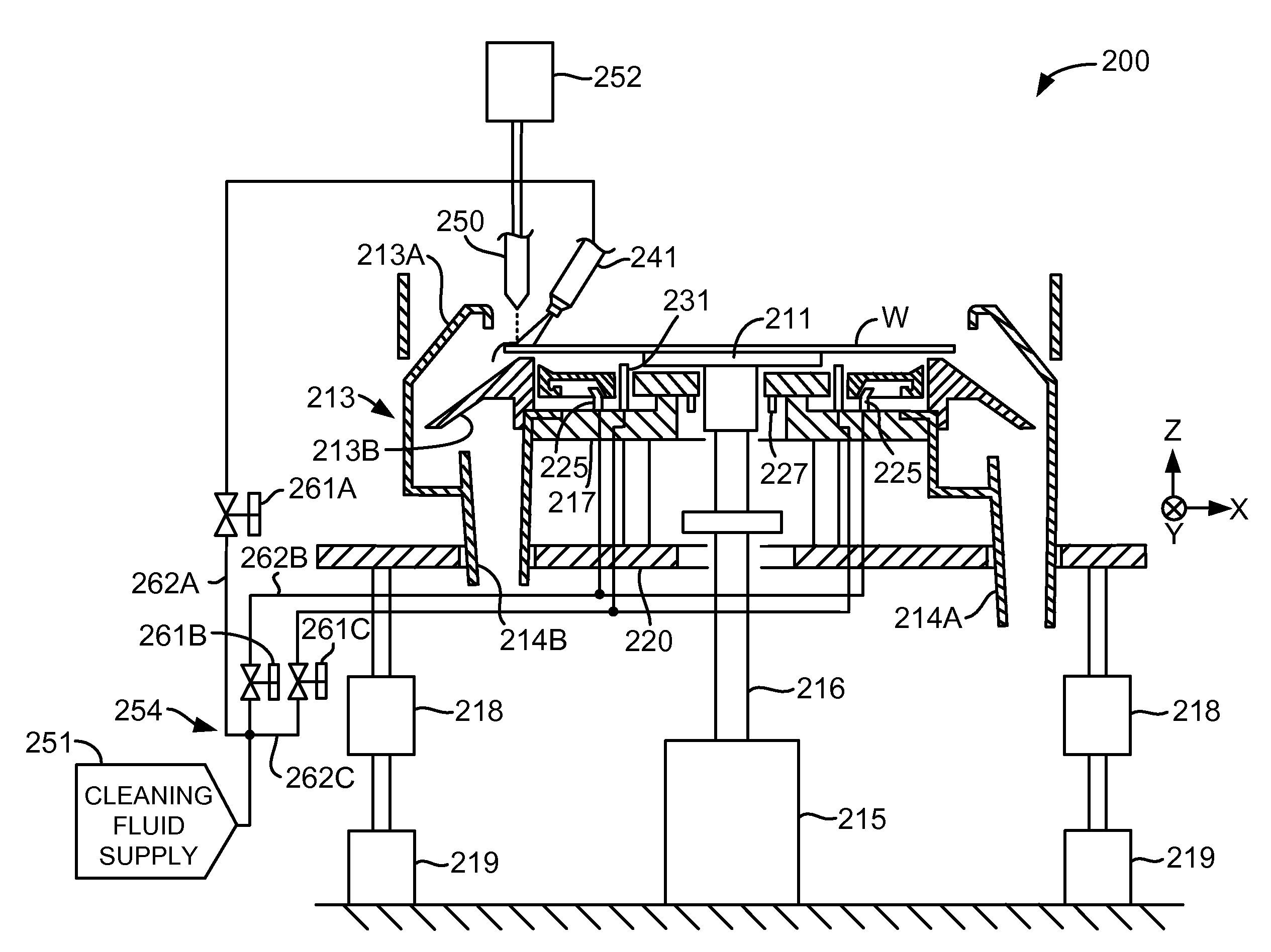
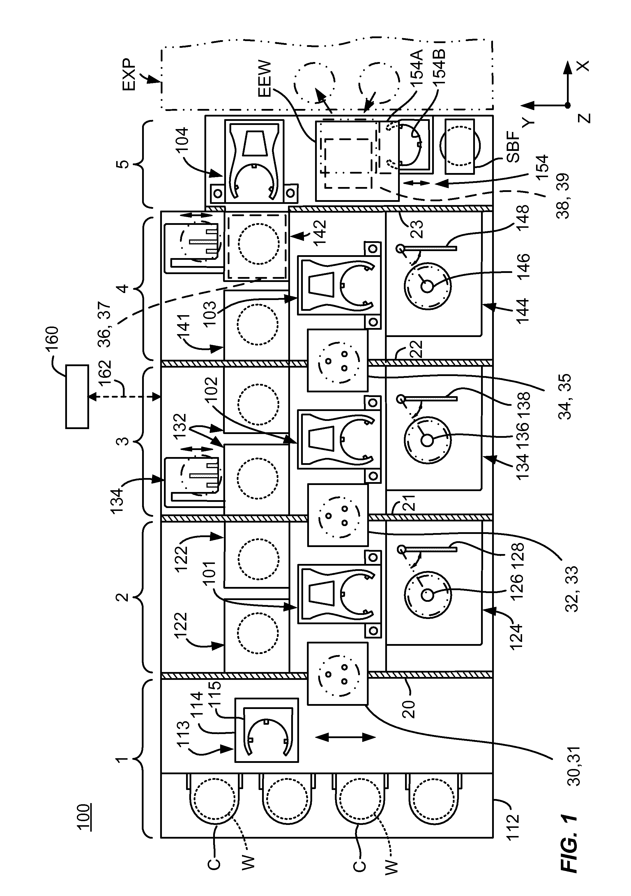
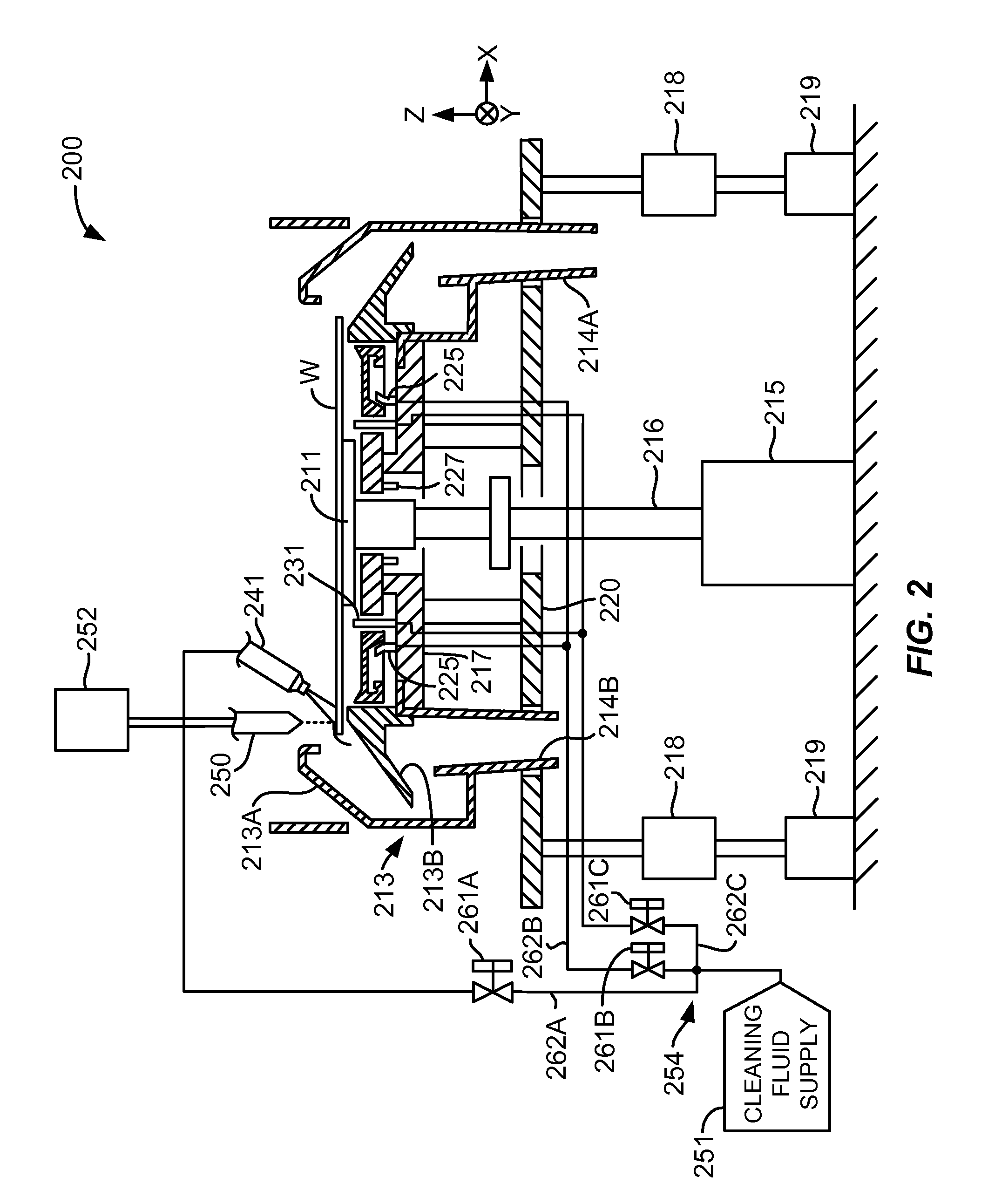
[0015]FIG. 1 is a plan view of a track lithography tool according to an embodiment of the present invention. In the embodiment illustrated in FIG. 1, the track lithography tool is coupled to an immersion scanner. An XYZ rectangular coordinate system in which an XY plane is defined as the horizontal plane and a Z axis is defined to extend in the vertical direction is additionally shown in FIG. 1 for purposes of clarifying the directional relationship therebetween.

[0016]In a particular embodiment, the track lithography tool is used to form, through use of a coating process, an anti-reflection (AR) and a photoresist film on substrates, for example, semiconductor wafers. The track lithography tool is also used to perform a development process on the substrates after they have been subjected to a pattern exposure process. The substrates processed by the track lithography tool are not limited to semiconductor wafers, but may include glass substrates for a liquid crystal display device, an...


PUM

PropertyMeasurementUnit
radial distanceaaaaaaaaaa

Abstract

An apparatus for processing a peripheral portion of a substrate includes a housing and a spin chuck mounted within the housing and configured to support the substrate in a substantially horizontal orientation. The apparatus also includes a fluid dispense nozzle coupled to the housing and proximate to the peripheral portion of the substrate. The fluid dispense nozzle is in fluid communication with a source of a chemical and configured to direct a flow of the chemical to the peripheral portion of the substrate located at a first radial distance from a center of the substrate. The apparatus further includes a light guide optically coupled to a laser source. The light guide is configured to direct radiation to the peripheral portion of the substrate located at a second radial distance from the center of the substrate greater than the first radial distance.

Description

BACKGROUND OF THE INVENTION[0001]The present invention relates generally to the field of substrate processing equipment. More particularly, the present invention relates to a method and apparatus for removing films on a substrate. In a particular embodiment, the method and system are applied to create a predetermined edge stack profile for layers present on a semiconductor wafer. However, embodiments of the present invention are also applicable to other substrate processing procedures, including substrate cleaning, resist trimming, and the like.[0002]Modern integrated circuits contain millions of individual elements that are formed by patterning the materials, such as silicon, metal and / or dielectric layers, that make up the integrated circuit to sizes that are small fractions of a micrometer. The technique used throughout the industry for forming such patterns is photolithography. A typical photolithography process sequence generally includes depositing one or more uniform photores...

Claims


Application Information

Patent Timeline
Patent Type & Authority Applications(United States)
IPC IPC(8): B08B7/04
CPCB08B7/0042H01L21/6708H01L21/67051H01L21/02087
Inventor ISHIKAWA, TETSUYAMITSUHASHI, TSUYOSHIXI, MING
Owner SOKUDO CO LTD
Why Eureka
Try Eureka