

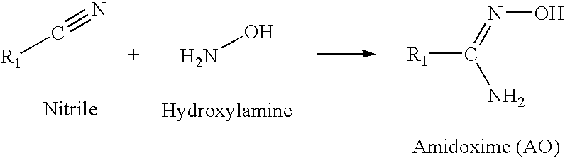
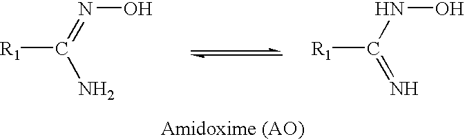
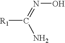
Amidoxime compounds as chelating agents in semiconductor processes
a technology of amidoxime compounds and semiconductors, applied in the field of amidoxime compounds as chelating agents in semiconductor processes, can solve the problems of unsatisfactory biodegradability of complexing agents, particle removal may not be the main objective, and the need for cleaning needs and goals have become more demanding, so as to achieve the effect of effectively removing surface residues and contaminants
- Summary
- Abstract
- Description
- Claims
- Application Information
AI Technical Summary
Benefits of technology
Problems solved by technology
Method used
Image

Examples
examples of embodiments
of the Present Invention
Exemplary Embodiments of the Present Invention
[0117]All patents and other published documents cited in the specification are intended to be incorporated herein by reference in their entireties.
example 1
[0118]In an exemplary embodiment of the invention, organometallic and organosilicate residues remaining after a dry etch process from semiconductor substrates were removed. The substrate was exposed to a conditioning solution of phosphoric acid, hydrofluoric acid, and a carboxylic acid, such as acetic acid, which removed the remaining dry etch residues while minimizing removal of material from desired substrate features. The approximate proportions of the conditioning solution were typically 80 to 95 percent by weight of the amidoxime compound and acetic acid, 1 to 15 percent by weight phosphoric acid, and 0.01 to 5.0 percent by weight hydrofluoric acid. See, e.g., U.S. Pat. No. 7,261,835.
[0119]In another exemplary embodiment, the composition included from about 0.5% to about 24% by weight of at least one complexing agent with an amidoxime functional group with an aqueous semiconductor cleaning solution having a pH between about 1.5 and about 6 and comprising: at least about 75% by ...
example 2
[0120]Table 1 lists additional exemplary embodiments of the present invention where the formulations additionally include from about 0.5% to about 24% by weight of amidoxime compounds in aqueous semiconductor cleaning solutions. Such formulations may contain additional components consistent with this application such as surfactants, alkaline components, and organic solvents.
TABLE 1Exemplary Formulations with Chelating Agents for Use with AmidoximeCompoundsH3PO4 (wt %)Other Acidwt %2methanesulfonic1.472pyrophosphoric acid (PPA)3.02Fluorosicilic0.242Oxalic2.04Oxalic2.06Glycolic1.03Oxalic2.03Lactic2.04Lactic2.03Citric2.04Citric2.03PPA0.53Glycolic2.06Glycolic2.03PPA2.03PPA4.0
PUM
| Property | Measurement | Unit |
|---|---|---|
| temperature | aaaaa | aaaaa |
| time | aaaaa | aaaaa |
| temperature | aaaaa | aaaaa |
Abstract
Description
Claims
Application Information